
Formation method of fin field-effect transistor

A technology of fin field effect transistors and fins, which is applied to semiconductor devices, electrical components, circuits, etc., can solve complex problems, achieve the effects of saving production costs, improving device design redundancy, and simplifying the process

Active Publication Date: 2017-07-14
SEMICON MFG INT (SHANGHAI) CORP +1
View PDF3 Cites 4 Cited by
  • Summary
  • Abstract
  • Description
  • Claims
  • Application Information

AI Technical Summary

Problems solved by technology

[0005] However, in the prior art, when the fins in the fin field effect transistors to be formed have different critical dimensions (CD, Critical Dimension), they are usually formed by a more complicated process. Therefore, it is urgent to provide a new A method for forming a fin field effect transistor, forming fins with different critical dimensions, and the process steps are simple

Method used


Image

  • Formation method of fin field-effect transistor
  • Formation method of fin field-effect transistor
  • Formation method of fin field-effect transistor

Examples


Embodiment Construction

[0031] It can be seen from the background art that when the formed fins have different critical dimensions, the forming process of the fin field effect transistor provided by the prior art is complicated.

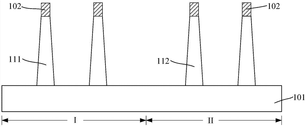
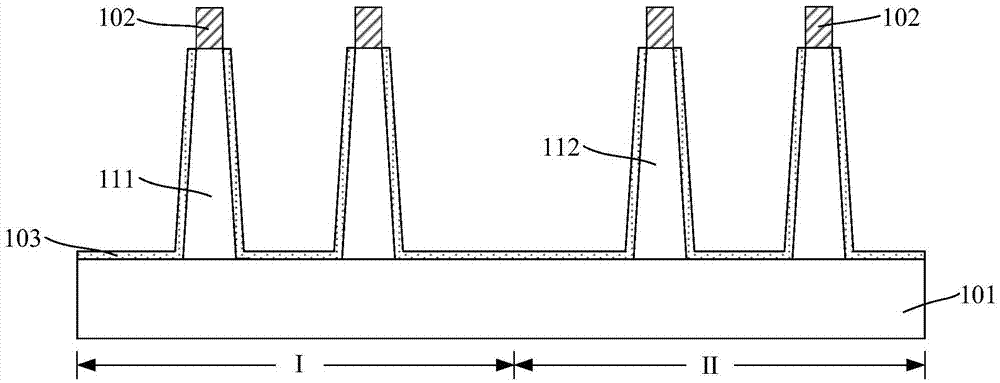
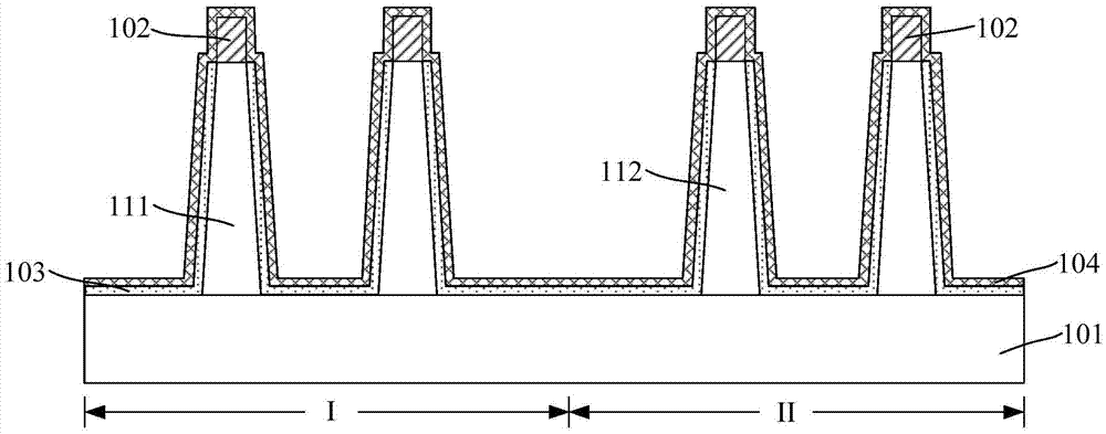
[0032] To this end, the present invention provides a method for forming a fin field effect transistor, providing a substrate including a first region and a second region, the substrate surface of the first region is formed with a first fin, and the second region A second fin is formed on the surface of the substrate, and the critical dimension of the first fin is the same as that of the second fin; forming a liner oxide layer on the surface of the wall; forming an insulating barrier layer on the surface of the liner oxide layer in the first region; A permanent precursor material layer, the top of the precursor material layer is higher than the top of the first fin and the top of the second fin; 2 Performing curing annealing treatment on the precursor material layer in an O...


PUM


Abstract

A formation method of a fin field-effect transistor comprises the steps of forming lining oxide layers on a surface, a surface of a side wall of a first fin part and a surface of a side wall of a second fin part; forming an insulation blocking layer on a surface of the lining oxide layer on a first region; depositing a precursor material layer on a surface of the insulation blocking layer and a surface of the lining oxide layer on a second region; performing curing and annealing on the precursor material layer under a H2O-containing atmosphere, and converting the precursor material layer to an insulation layer, wherein during the curing and annealing process, the side wall of the first fin part is oxidized to form a first oxide layer, the side wall of the second fin part is oxidized to form a second oxide layer, and the thickness of the first oxide layer is smaller than the thickness of the second oxide layer; and removing the insulation layer in a partial thickness to form an isolation layer, and also removing the lining oxide layer, the insulation blocking layer, the first oxide layer and the second oxide layer which are higher than the top of the isolation layer. After the isolation layer is formed, the critical dimension of the first fin part is larger than the critical dimension of the second fin part, and the process is simple in step.

Description

technical field [0001] The invention relates to the technical field of semiconductor manufacturing, in particular to a method for forming a fin field effect transistor. Background technique [0002] With the continuous development of semiconductor process technology, the development trend of semiconductor process nodes following Moore's Law continues to decrease. In order to adapt to the reduction of process nodes, the channel length of MOSFET field effect transistors has to be continuously shortened. The shortening of the channel length has the advantages of increasing the die density of the chip and increasing the switching speed of the MOSFET field effect tube. [0003] However, as the channel length of the device is shortened, the distance between the source and the drain of the device is also shortened, so that the control ability of the gate to the channel becomes worse, and the gate voltage pinches off the channel. The difficulty is also increasing, making the pheno...

Claims


Application Information

Patent Timeline
Patent Type & Authority Applications(China)
IPC IPC(8): H01L21/8234
CPCH01L21/823431H01L27/0886H01L21/31053H01L21/31111H01L21/31144H01L21/324H01L29/0649H01L29/66795H01L29/785
Inventor 毛刚
Owner SEMICON MFG INT (SHANGHAI) CORP
Learn More