SiO2 doped Sb nano phase change film material, and preparation method and application of film material

A technology of thin film materials and nano phases, which is applied in the field of materials in the field of microelectronics technology, can solve problems such as poor thermal stability, slow phase transition speed, and easy pollution, and achieve good stability, good uniformity, and simple preparation methods.

Inactive Publication Date: 2017-07-14
JIANGSU UNIV OF TECH
View PDF7 Cites 8 Cited by
  • Summary
  • Abstract
  • Description
  • Claims
  • Application Information

AI Technical Summary

Problems solved by technology

[0007] The purpose of the present invention is to overcome the technical problems of poor thermal stability, slow phase change speed and easy pollution o...

Method used


Image

  • SiO2 doped Sb nano phase change film material, and preparation method and application of film material
  • SiO2 doped Sb nano phase change film material, and preparation method and application of film material
  • SiO2 doped Sb nano phase change film material, and preparation method and application of film material

Examples


Embodiment 1

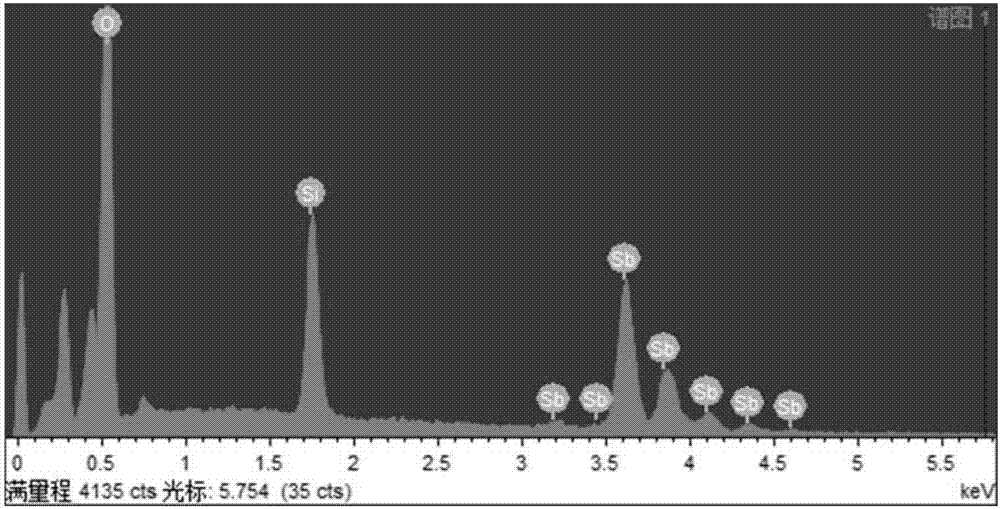
[0043] (SiO prepared in this example 2 ) x Sb 1-x The structure of the nano phase change thin film material is specifically (SiO 2 ) 0.22 Sb 0.78 , the preparation steps are:

[0044] 1. Clean SiO2 2 / Si(100) substrate, remove dust particles, organic and inorganic impurities, clean the surface and back;

[0045] a) strong ultrasonic cleaning in ethanol solution for 10-15 minutes, and rinse with deionized water;

[0046] b) Strong ultrasonic cleaning in acetone solution for 10-15 minutes, rinse with deionized water, high-purity N 2 Blow dry the surface and back;

[0047] c) Dry the water vapor in an oven at 120°C for about 30 minutes.

[0048] 2. Prepared by radio frequency magnetron sputtering (SiO 2 ) 0.22 Sb 0.78 Film preparation:

[0049] a) Install the Sb sputtering target, and place SiO with a diameter of 10mm 2 The target sheet is stacked in the center of the Sb target to form a composite target, hereinafter referred to as (SiO 2 ) x Sb 1-x . Sb and SiO...

Embodiment 2

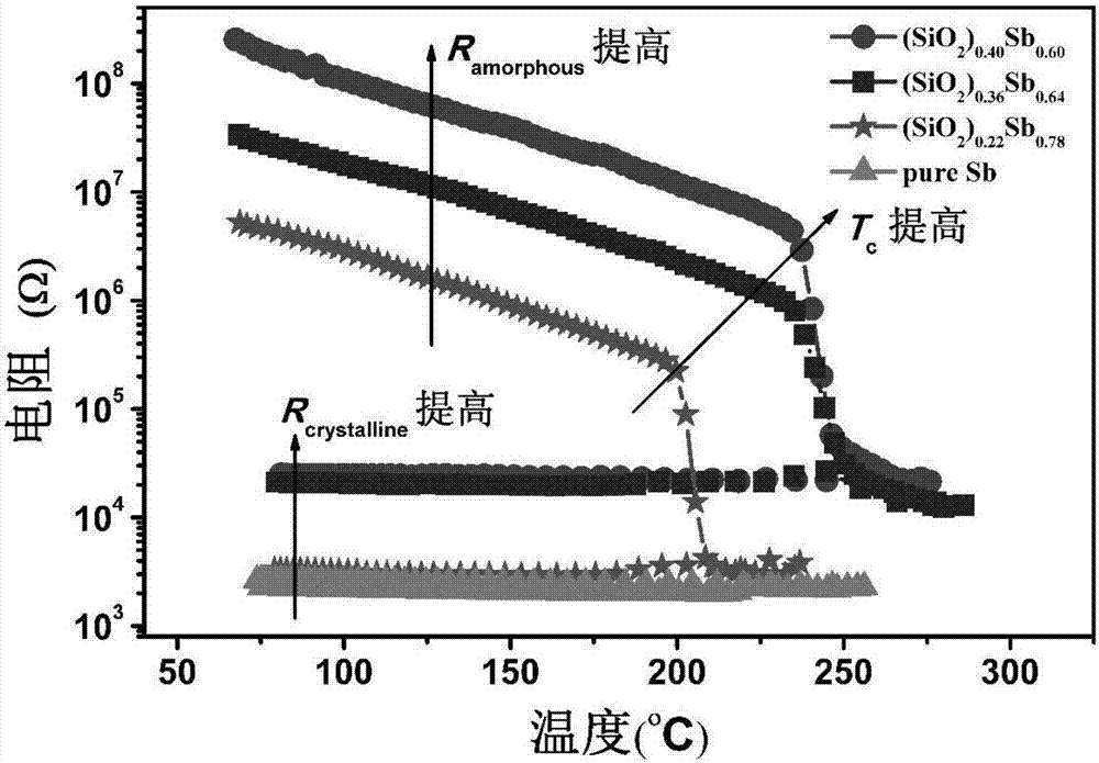
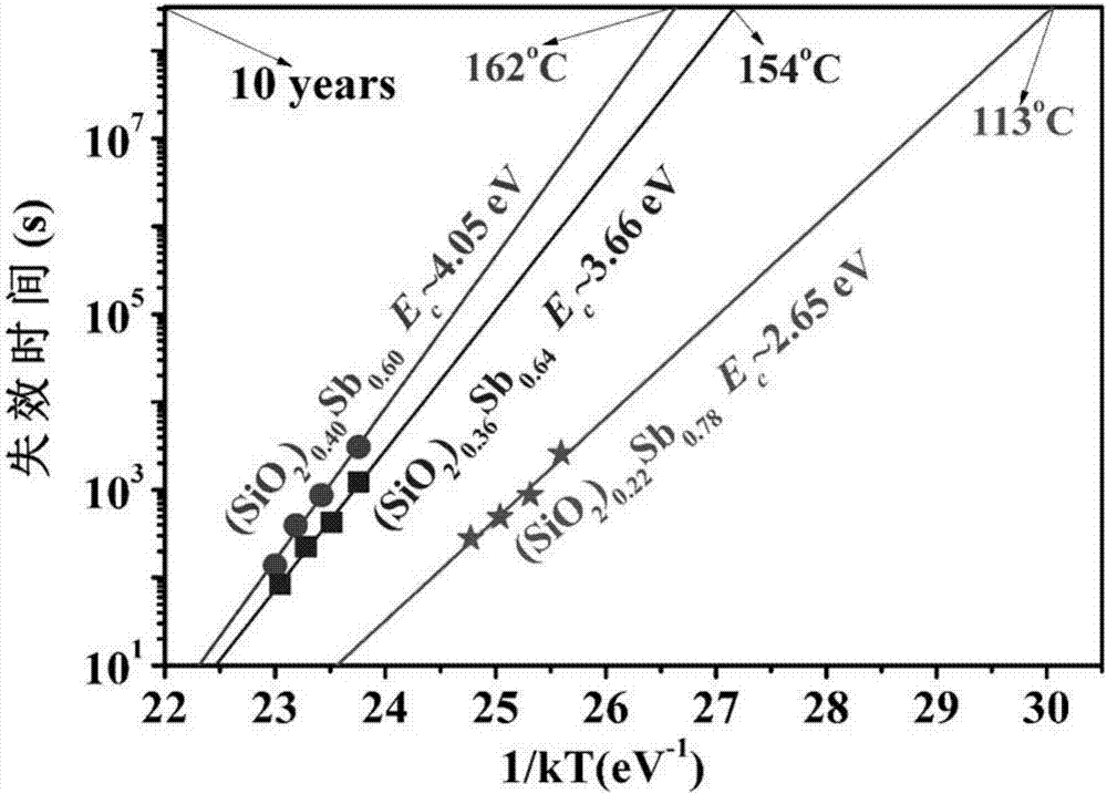
[0057] Prepared in this example (SiO 2 ) x Sb 1-x The specific structures of the nano phase change thin film materials are (SiO 2 ) 0.36 Sb 0.64 and (SiO 2 ) 0.40 Sb 0.60 , and the (SiO 2 ) 0.36 Sb 0.64 and (SiO 2 ) 0.40 Sb 0.60 The thickness of the nano phase change thin film material is 50nm.

[0058] The above (SiO 2 ) 0.36 Sb 0.64 and (SiO 2 ) 0.40 Sb 0.60 The preparation method of nanometer phase-change film material is identical with embodiment 1, only in the SiO that uses 2 There is a difference in sheet diameter, (SiO 2 ) 0.36 Sb 0.64 and (SiO 2 ) 0.40 Sb 0.60 The circular SiO used 2 The diameters of the sheets were 20 mm and 30 mm, respectively.


PUM

PropertyMeasurementUnit
Thicknessaaaaaaaaaa
Diameteraaaaaaaaaa

Abstract

The invention discloses an SiO2 doped Sb nano phase change film material, and a preparation method and an application of the film material. A chemical composition of the SiO2 doped Sb nano phase change film material is (SiO2)xSb1-x, wherein x is greater than or equal to 0.22 and less than or equal to 0.40; and the film material is deposited by a magnetron sputtering method. The prepared SiO2 doped Sb nano phase change film material has a high crystallization temperature, can effectively improve thermal stability of a PCRAM (Phase Change Random Access Memory), has a high crystallization speed, and can greatly increase a memory speed of the PCRAM.

Description

technical field [0001] The invention relates to materials in the technical field of microelectronics, in particular to a SiO 2 Doped Sb nano phase change thin film material and its preparation method and application. Background technique [0002] Phase change memory (PCRAM) has the advantages of low power consumption, strong stability, fast reading speed, high storage density, and compatibility with traditional CMOS processes, so it has attracted more and more researchers' attention and has become the most potential One of the next generation non-volatile data storage. As an important part of phase change memory, the performance of phase change material plays a vital role in phase change memory. The Joule heat generated by the electric pulse can realize the reversible transition between the crystalline state and the amorphous state of the phase change material. When the phase change material is in the amorphous state, it has high resistance, and when it is in the crystalli...

Claims


Application Information

Patent Timeline
IPC IPC(8): H01L45/00B82Y30/00B82Y40/00
CPCB82Y30/00B82Y40/00H10N70/881H10N70/026H10N70/8833
Inventor 胡益丰朱小芹尤海鹏袁丽邹华张剑豪孙月梅薛建忠吴世臣吴卫华郑龙翟良君
Owner JIANGSU UNIV OF TECH
Why Eureka
Try Eureka