Thin film transistor array panel
A technology of thin film transistors and array substrates, applied in the field of thin film transistor array substrates, can solve problems affecting device performance, poor structure, etc., and achieve good electrical effects
- Summary
- Abstract
- Description
- Claims
- Application Information
AI Technical Summary
Problems solved by technology
Method used
Image


Examples
Embodiment Construction
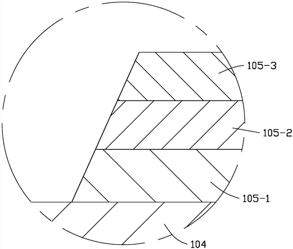
[0025] figure 1 It is a schematic layout diagram of a thin film transistor array substrate in a preferred embodiment of the present invention. figure 1 A TFT array substrate is disclosed, which includes a plurality of pixel units 10 arranged to form a matrix with multiple rows and multiple columns. Each pixel unit 10 includes at least one TFT element 100 and at least one pixel electrode 120 . The TFT element 100 is a transistor with low field effect and is composed of a semiconductor thin film, a conductive thin film and a dielectric layer. The thin films of different materials are usually arranged on a supporting structure (such as an insulating substrate 101 ). Each TFT element 100 includes a gate 102 and a pair of mutually switchable source 1051 and drain 1052 . The pixel electrodes 120 are used in the display to drive liquid crystals (not shown). The pixel electrode 120 is connected to the source 1051 or the drain 1052 of the TFT element 100 . The TFT element 100 acts ...
PUM
| Property | Measurement | Unit |
|---|---|---|
| Angle | aaaaa | aaaaa |
Abstract
Description
Claims
Application Information