

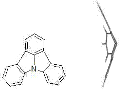
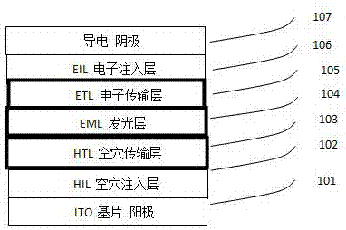
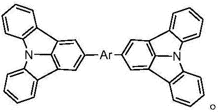
Indolocarbazole-containing organic semiconductor material and application thereof to organic luminous device
An organic semiconductor and organic technology, applied in the application field of organic electroluminescence devices, can solve the problems of limited material performance improvement and low yield.
- Summary
- Abstract
- Description
- Claims
- Application Information
AI Technical Summary
Problems solved by technology
Method used
Image

Examples
Embodiment 1
[0113] Example 1: Synthesis and preparation of compound 7C host material:
[0114] Compound 7C was prepared according to the following chemical synthesis route, and a white powder material was obtained, PL=415nm. The molecular structure was verified by mass spectrometry as shown in Table 11.
[0115]
Embodiment 2
[0116] Example 2: Synthesis and preparation of compound 18C hole transport material:
[0117] Compound 18C was prepared according to the following chemical synthesis route, a white powder material was obtained, PL=420nm, and the molecular structure was verified by mass spectrometry as shown in Table 11.
[0118]
Embodiment 3
[0119] Example 3: Synthesis and preparation of compound X-6 electron transport material:
[0120] Compound X-6 was prepared according to the following chemical synthesis route, a white powder material was obtained, PL=440nm, and the molecular structure was verified by mass spectrometry as shown in Table 9.
[0121]
PUM
| Property | Measurement | Unit |
|---|---|---|
| thickness | aaaaa | aaaaa |
Abstract
Description
Claims
Application Information