A compact photonic structure based on microring cavity to realize multiple resonance line shapes
A technology of photonic structure and microring, applied in the coupling of optical waveguide, etc., can solve the problem of insufficient compactness, and achieve the effect of small processing error, compact photonic structure, and low processing technology requirements
- Summary
- Abstract
- Description
- Claims
- Application Information
AI Technical Summary
Problems solved by technology
Method used
Image
Examples
Embodiment Construction
[0029] Now in conjunction with embodiment, accompanying drawing, the present invention will be further described:
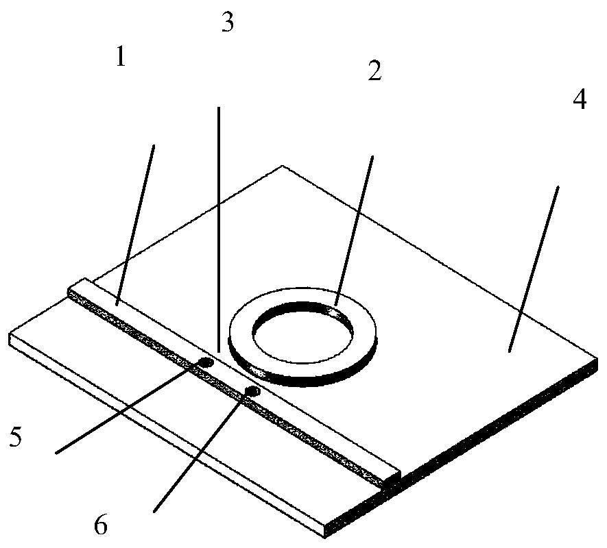
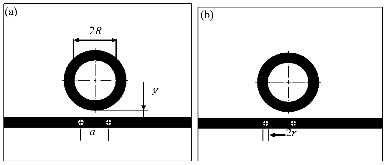
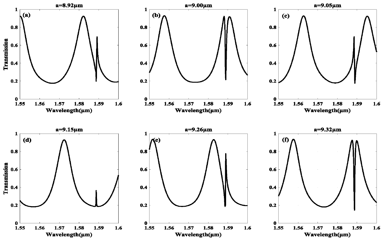
[0030] The embodiment of the present invention proposes a compact photonic structure based on a microring cavity to realize multiple resonance line types, such as figure 1 As shown in Fig. 1, the structure is based on the traditional micro-ring cavity side-coupled straight waveguide structure, and two air holes are dug out in the straight waveguide. Two air holes can be distributed symmetrically about the microring cavity figure 2 (a), also available off-centre figure 2 (b).
[0031] The materials used for the straight waveguide 1 and the micro-ring cavity 2 are generally high refractive index or have a high refractive index relative to its substrate and cladding, and there are group IV materials such as silicon, silicon nitride, silicon oxynitride, etc., III-V semiconductor materials such as gallium phosphide, lithium niobate, and certain polymers such as p...
PUM
 Abstract
Description
Claims
Application Information


