MOS tube parameter degradation circuit and MOS tube parameter degradation early warning circuit

A technology of parameter degradation and MOS tube, applied in the field of monitoring, can solve problems such as inability to accurately analyze the degree of device parameter degradation, reduce the accuracy of early warning signals, and inaccurate output signals

Active Publication Date: 2017-08-11
CHINA ELECTRONICS PROD RELIABILITY & ENVIRONMENTAL TESTING RES INST
View PDF4 Cites 6 Cited by
  • Summary
  • Abstract
  • Description
  • Claims
  • Application Information

AI Technical Summary

Problems solved by technology

[0004] At this stage, the research on the NBTI effect is mainly focused on the performance degradation of integrated circuits. Among them, in the monitoring circuit of the device parameter degradation characteristics caused by the NBTI effect, due to the fact that the circuit will be subjected to HCI (hot carrier injection, hot carrier injection) while the circuit is working ), NBTI and TDDB (time dependent dielectric brea...

Method used


Image

  • MOS tube parameter degradation circuit and MOS tube parameter degradation early warning circuit
  • MOS tube parameter degradation circuit and MOS tube parameter degradation early warning circuit
  • MOS tube parameter degradation circuit and MOS tube parameter degradation early warning circuit

Examples


Embodiment Construction

[0036] In order to further explain the technical means adopted by the present invention and the effects obtained, the technical solutions of the embodiments of the present invention will be clearly and completely described below in conjunction with the accompanying drawings and preferred embodiments.

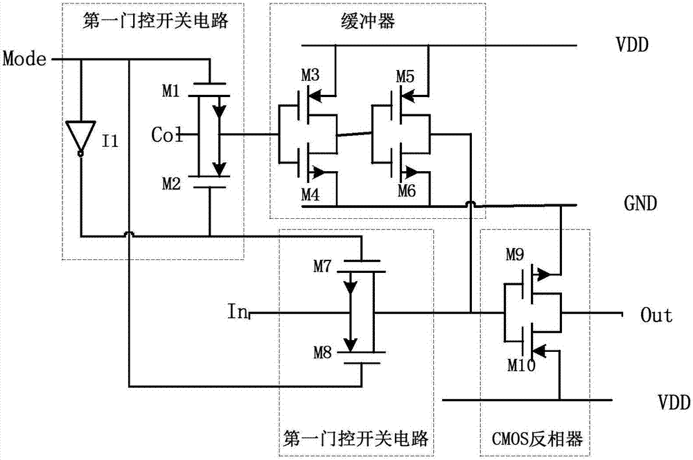
[0037] See figure 1 and figure 2 , a MOS transistor parameter degradation circuit, including a CMOS inverter, a stress application circuit and a parameter measurement circuit; the CMOS inverter includes a first PMOS transistor M10 and a first NMOS transistor M9; the first PMOS transistor M10 The gate is connected to the gate of the first NMOS transistor M9 as the input end of the CMOS inverter; the drain of the first PMOS transistor M10 is connected to the drain of the first NMOS transistor as the input end of the CMOS inverter. The output end of the CMOS inverter; the source of the first PMOS transistor M10 is connected to the power supply VDD, and the source of the first NMO...


PUM


Abstract

The invention relates to a MOS tube parameter degradation circuit, which comprises a CMOS inverter, a stress applying circuit and a parameter measuring circuit. The CMOS inverter comprises a first PMOS tube and a first NMOS tube. The stress applying circuit becomes on under the control of a first mode-select signal. After the stress applying circuit receives a control signal, it exerts negative gate voltage bias stress or positive gate voltage bias stress on the first PMOS tube of the CMOS inverter. The parameter measuring circuit becomes on under the control of a second mode-select signal. The parameter measuring circuit receives an input signal and transmits the input signal to the input end of the CMOS inverter. The first mode-select signal and the second mode-select signal are compensation signals. With the invention, it is possible to make the MOS tube parameter degradation testing result more accurate. In addition, the invention also relates to a MOS tube parameter degradation early warning circuit, which can accurately analyze the influence of NBTI effect on PMOS tube component parameters.

Description

technical field [0001] The invention relates to the technical field of monitoring, in particular to a MOS tube parameter degradation circuit, a MOS tube parameter degradation early warning circuit, and another MOS tube parameter degradation early warning circuit. Background technique [0002] NBTI (Negative Bias Temperature Instability, negative bias temperature instability) effect refers to the PMOS (positive channel Metal Oxide Semiconductor, n-type substrate, p-channel, relying on holes) under high temperature and negative gate voltage bias stress The flow of the field effect transistor that carries the current) The degradation effect of the tube, that is, under the influence of the NBTI effect, will cause the threshold voltage of the PMOS tube of the device to drift, and the drain saturation current and transconductance will all decrease, resulting in the device and even the entire Circuit failure. [0003] At present, high-performance CMOS (Complementary Metal Oxide Se...

Claims


Application Information

Patent Timeline
IPC IPC(8): H01L21/66H01L23/544G01R31/26
CPCG01R31/2621H01L22/14H01L22/34
Inventor 恩云飞雷登云陈义强何春华黄云
Owner CHINA ELECTRONICS PROD RELIABILITY & ENVIRONMENTAL TESTING RES INST
Why Eureka
Try Eureka