Array substrate and preparation method thereof, display panel and display device

A technology for array substrates and display panels, which is applied in the manufacture of semiconductor/solid-state devices, electrical components, and electrical solid-state devices, etc., can solve problems such as reducing the aperture ratio of display devices and affecting the display quality of display panels.

Inactive Publication Date: 2017-08-11
BOE TECH GRP CO LTD +1
View PDF6 Cites 15 Cited by
  • Summary
  • Abstract
  • Description
  • Claims
  • Application Information

AI Technical Summary

Problems solved by technology

However, the comparison of the area of ​​the second electrode 2 of the storage capacitor Cst will ser...

Method used


Image

  • Array substrate and preparation method thereof, display panel and display device
  • Array substrate and preparation method thereof, display panel and display device
  • Array substrate and preparation method thereof, display panel and display device

Examples


preparation example Construction

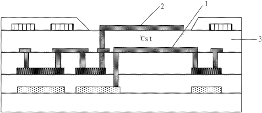
[0049] Based on the same inventive concept, an embodiment of the present invention also provides a method for preparing an array substrate, such as Figure 4 shown, including:

[0050] S401, forming a driving transistor and a switching transistor on a base substrate, and forming a pattern of a first electrode of a first capacitor, wherein the first electrode of the first capacitor is respectively connected to a gate electrode of the driving transistor and a source electrode of the switching transistor;

[0051] S402, forming a pattern of a passivation layer covering the first electrode of the first capacitor, and the passivation layer is provided with a groove and a via hole penetrating through the passivation layer in a region corresponding to the first electrode of the first capacitor;

[0052] S403, forming a pattern of the second electrode of the first capacitor in the groove, and connecting the second electrode of the first capacitor to the source of the driving transisto...

Embodiment 1

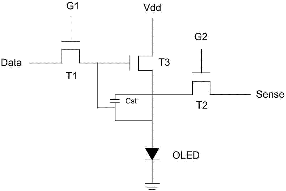
[0056] Taking an array substrate including 3 transistors and 1 capacitor as an example, the preparation method of the array substrate specifically includes:

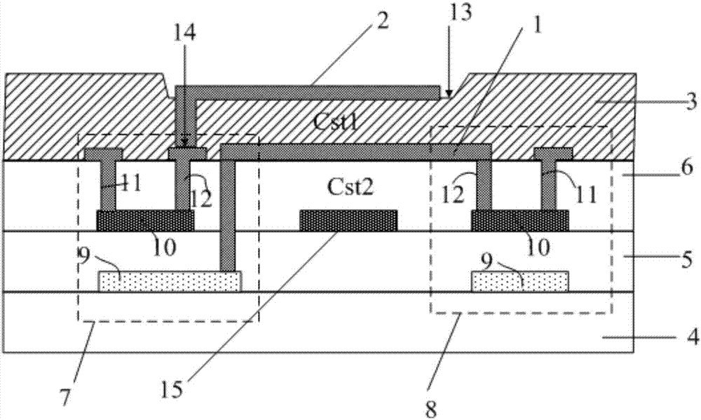
[0057] 1. A gate electrode 9, a gate insulating layer 5, an active layer 10, an etching stopper layer 6, a drain electrode 11 or a source electrode 12, and a passivation layer 3 are sequentially formed on the base substrate 4 through a patterning process, such as Figure 5a shown;

[0058] 2. Coating photoresist 16 above the passivation layer 3, such as Figure 5b shown;

[0059] 3. Irradiating the photoresist 16 with a half-tone mask or a gray-tone mask to form a via area corresponding to the I region and a groove region corresponding to the II region on the photoresist 16, wherein the half-tone mask The slab or gray tone mask includes a transparent area I, a semi-transparent area II and a light-shielding area III, such as Figure 5c shown;

[0060] 4. Form a via hole 14 penetrating through the passivation layer at ...


PUM


Abstract

The present invention discloses an array substrate and a preparation method thereof, a display panel and a display device. The array substrate comprises a pixel circuit located on a substrate, and the pixel circuit at least comprises a driving transistor, a switch transistor and a first capacitor; the first electrode of the first capacitor is connected with the gate electrode of the driving transistor and the source of the switch transistor; the array substrate also comprises a passivation layer covering the first electrode of the first capacitor, the passivation layer is provided with a second electrode of the first capacitor in a groove arranged at an area corresponding to the first electrode of the first capacitor compared to that the second electrode is arranged on the passivation layer, the distance between the first electrode and the second electrode is reduced, and the storage content of the capacitor is increased so as to realize arrangement of a small electrode area while ensuring the capacitor storage, increase the aperture ratio of the array substrate and add the display quality.

Description

technical field [0001] The invention relates to the field of display technology, in particular to an array substrate and a preparation method, a display panel and a display device. Background technique [0002] Active Matrix Organic Light-Emitting Diode (AM-OLED) has a series of advantages such as self-illumination, high brightness, wide viewing angle, high contrast ratio, and low power consumption, and has attracted widespread attention. [0003] like figure 1 As shown, the existing AM-OLED array substrate generally adopts the driving mode of 3T1C, that is, each sub-pixel is driven by three thin film transistors (Thin Film Transistor, TFT) and one storage capacitor Cst. The switch tube T1 stores the Data signal in the storage capacitor Cst, the compensation tube T2 provides a compensation current to the drive tube T3, and the drive tube T3 supplies current to the OLED to drive the AM-OLED to emit corresponding light. Normally, the storage capacitor Cst is large enough to ...

Claims


Application Information

Patent Timeline
IPC IPC(8): H01L27/12H01L27/32H01L21/77
CPCH01L27/1255H01L27/1259H10K59/1216
Inventor 苏同上王东方刘军成军袁广才
Owner BOE TECH GRP CO LTD
Why Eureka
Try Eureka