Image sensor pixel unit and manufacturing method thereof

An image sensor and pixel unit technology, applied in the field of image sensors, can solve the problem that the gate cannot effectively control the electron transmission, short channel effect, etc. Effect

Active Publication Date: 2020-03-31
SHANGHAI INTEGRATED CIRCUIT RES & DEV CENT
View PDF3 Cites 0 Cited by
  • Summary
  • Abstract
  • Description
  • Claims
  • Application Information

AI Technical Summary

Problems solved by technology

More importantly, in the process of shrinking the device size in order to integrate more pixel units, due to the reduction of the physical gate length of the transfer transistor with a planar structure, the short channel effect or punch-through occurs, and the gate cannot effectively control the transmission of electrons.

Method used


Image

  • Image sensor pixel unit and manufacturing method thereof
  • Image sensor pixel unit and manufacturing method thereof
  • Image sensor pixel unit and manufacturing method thereof

Examples


Embodiment Construction

[0032] In order to make the content of the present invention clearer and easier to understand, the content of the present invention will be further described below in conjunction with the accompanying drawings. Of course, the present invention is not limited to this specific embodiment, and general replacements known to those skilled in the art are also covered within the protection scope of the present invention.

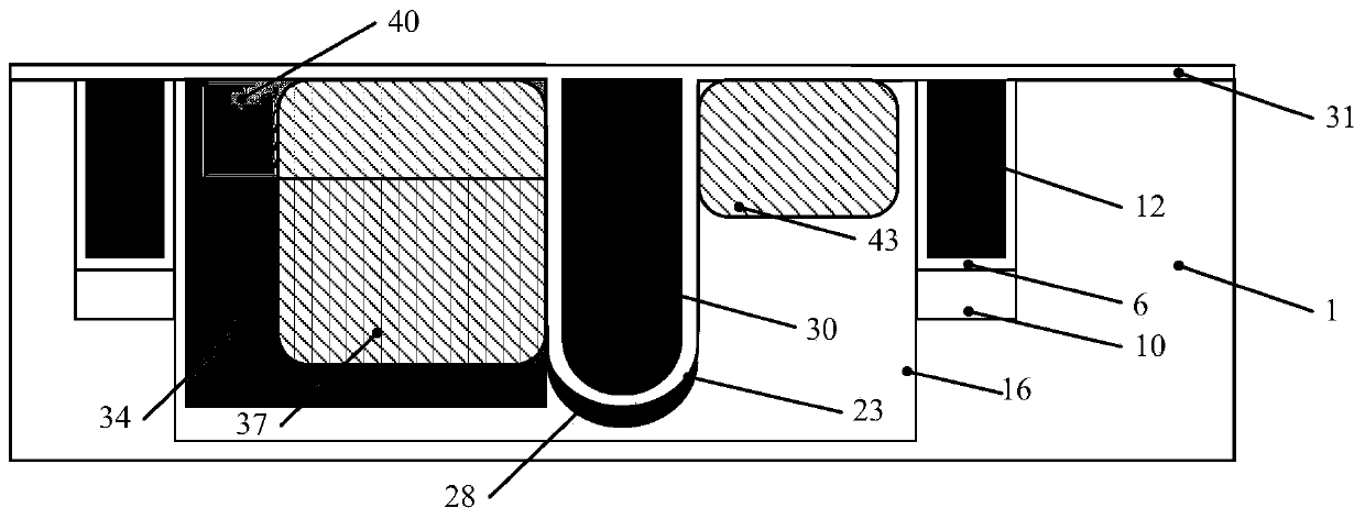
[0033] See figure 1 , which is a schematic diagram of an image sensor pixel unit according to an embodiment of the present invention. The image sensor pixel unit includes photodiodes 34, 37, a transfer transistor, a floating diffusion, and a readout circuit (not shown) connected to the floating diffusion. As shown in the figure, the transfer transistor has a trench gate, the bottom of the trench gate has an outwardly convex arc-shaped structure, and an arc-shaped channel region 23 is formed along the bottom of the arc-shaped structure. By changing the planar gate...


PUM

PropertyMeasurementUnit
electrical resistivityaaaaaaaaaa
thicknessaaaaaaaaaa
thicknessaaaaaaaaaa

Abstract

The invention discloses an image sensor pixel unit. The image sensor pixel unit comprises photoelectric diodes, a transmission transistor, a floating diffusion region and a readout circuit connected to the floating diffusion region, wherein the transmission transistor has a slot gate; an arc-shaped structure which is convex outwards is arranged at the bottom of the slot gate; and an arc-shaped channel region is formed along the bottom of the arc-shaped structure. The invention also provides a manufacturing method for the image sensor pixel unit; and the transmission transistor gate length can be greatly improved while the short channel effect and the punchthrough effect of a device can be improved consequently.

Description

technical field [0001] The present invention relates to the technical field of image sensors, in particular to an image sensor pixel unit and a manufacturing method thereof. Background technique [0002] An image sensor refers to a device that converts optical signals into electrical signals, and is an important part of a digital camera. According to the different components, it can be divided into two categories: CCD (Charge Coupled Device, charge coupled device) and CMOS (Complementary Metal-Oxide Semiconductor, metal oxide semiconductor device). Generally, for a CCD or CIS common image sensor, each pixel unit includes a photodiode PD, a transfer transistor, a row gate transistor, a reset transistor, and a source follower transistor. Wherein, at the source end of the transfer transistor is a photodiode, which is used to convert the collected optical signal into an electrical signal (electrons); at the drain end of the transfer transistor is a floating diffusion region, an...

Claims


Application Information

Patent Timeline
Patent Type & Authority Patents(China)
IPC IPC(8): H01L27/146
CPCH01L27/14603H01L27/14643H01L27/14683
Inventor 龟井诚司
Owner SHANGHAI INTEGRATED CIRCUIT RES & DEV CENT
Why Eureka
Try Eureka