Semiconductor device and manufacturing method thereof

A manufacturing method and semiconductor technology, applied in semiconductor devices, semiconductor/solid-state device manufacturing, transistors, etc., can solve the problem of inability to control the switching of semiconductor devices alone

Active Publication Date: 2020-12-08
INST OF MICROELECTRONICS CHINESE ACAD OF SCI
View PDF2 Cites 0 Cited by
  • Summary
  • Abstract
  • Description
  • Claims
  • Application Information

AI Technical Summary

Problems solved by technology

[0004] The main purpose of the present application is to provide a semiconductor device and its manufacturing method to solve the problem in the prior art that the switch of a semiconductor device formed of a certain two-dimensional semiconductor material cannot be individually controlled

Method used


Image

  • Semiconductor device and manufacturing method thereof
  • Semiconductor device and manufacturing method thereof
  • Semiconductor device and manufacturing method thereof

Examples


Embodiment 1

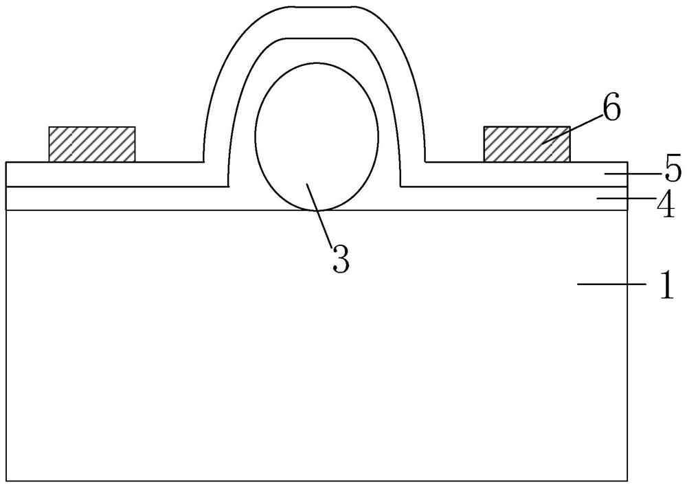
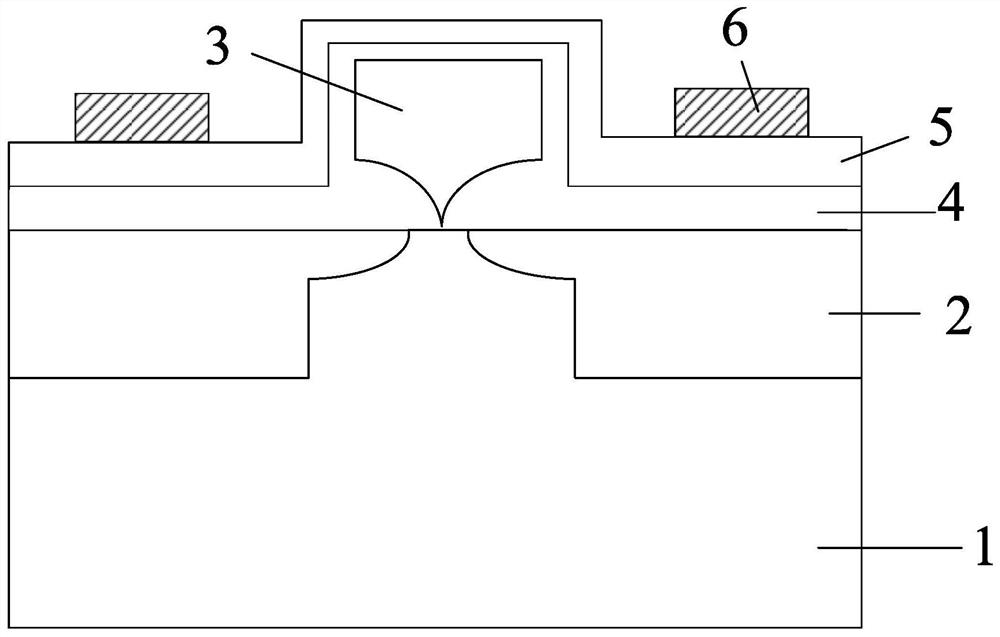
[0076] The specific travel process of semiconductor devices can be found in Figure 4 to Figure 10 . Specifically, the formation process includes:

[0077] First, a nanowire back gate is provided on a part of the surface of the substrate 1 .

[0078] A substrate is provided, which is a silicon substrate, and silicon is deposited on the surface of the substrate 1 to form a back gate material layer 30; the back gate material layer 30 and the substrate 1 are etched, so that the substrate 1 is formed as Figure 4 The structure shown includes a first part and a second part protruding from the first part, and the etched back gate material layer 30 is formed Figure 4 The first pre-structure 31 shown has depressions on both side walls at the junction of the first pre-structure 31 and the substrate 1; wet oxygen oxidation is used to oxidize the first pre-structure 31 and the substrate 1, so that the surface layers of both Form a dense silicon oxide surface layer, that is, the forma...

Embodiment 2

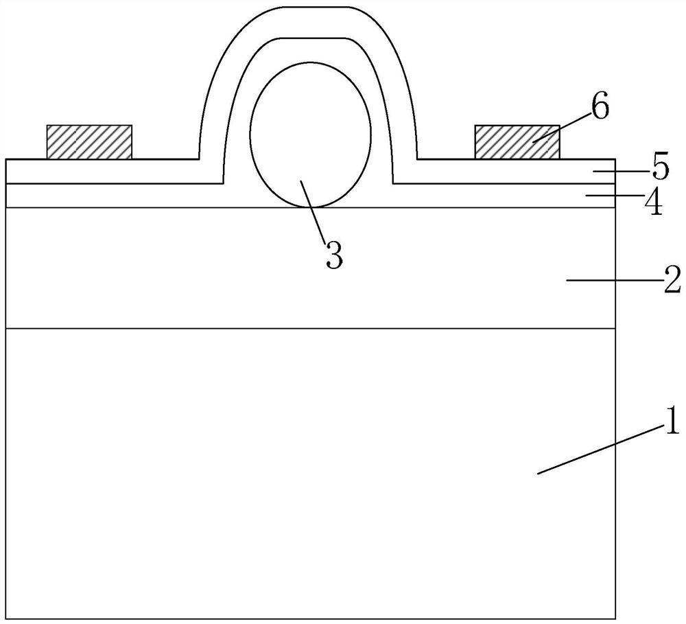
[0088] The specific travel process of semiconductor devices can be found in Figure 11 to Figure 15 . Specifically, the formation process includes:

[0089] First, a nanowire back gate is provided on a part of the surface of the substrate 1 .

[0090] A substrate 1 is provided, the substrate 1 is a silicon substrate, GeSi is deposited on the surface of the substrate 1 to form a sacrificial layer 13; silicon is deposited on the surface of the sacrificial layer 13 away from the substrate 1 to form a back gate material layer 30, Such as Figure 11 As shown; dry etching method is used to etch the sacrificial layer 13 and the back gate material layer 30 to form on the substrate 1 Figure 12 In the second pre-structure 32 shown, in fact, in the process of forming the back gate by etching, a support structure for supporting the back gate is formed at the same time, the support structure is located on both sides of the back gate and connected to the back gate, Figure 12 Not shown...


PUM

PropertyMeasurementUnit
heightaaaaaaaaaa
widthaaaaaaaaaa
thicknessaaaaaaaaaa

Abstract

The invention provides a semiconductor device and a manufacturing method therefor. The semiconductor device comprises a substrate, a back gate, a gate dielectric layer, a two-dimensional semiconductor material layer and two electrodes, wherein the back gate is arranged on a partial surface of the substrate; the gate dialectic layer is arranged on the exposed surface of the back gate; the two-dimensional semiconductor material layer is arranged on the surface, far from the back gate, of the gate dielectric layer; and the two electrodes are arranged on the surface, far from the gate dielectric layer, of the two-dimensional semiconductor material layer, and are arranged on the two sides of the back gate respectively. According to the semiconductor device, the back gate is arranged on the surface of the substrate; by applying different bias voltages on the back gate, different current carriers (such as electrons, holes and the like) can be induced through the electric field of the gate dielectric layer to enable a two-dimensional semiconductor material energy band to be bent; and by applying the bias voltages with proper values in source and drain regions, conductive channels can be switched on or pinched off to further realize on and off of the device in order to further realize independent control of the on and off of the device by the back gate, thereby satisfying the basic requirements of design of a large-scale integrated circuit.

Description

technical field [0001] The present application relates to the field of semiconductors, and in particular, to a semiconductor device and a manufacturing method thereof. Background technique [0002] Two-dimensional semiconductor materials with a single-layer structure (such as graphene, black phosphorus, graphyne, indium antimonide, indium phosphide, molybdenum sulfide, zinc sulfide, and silicene, etc.) have superior physical properties such as high carrier mobility And electrical properties, become the material that is most likely to replace silicon and is widely used in integrated circuits in the future. However, two-dimensional materials with a single-layer structure are very fragile, and their processing requirements are more stringent than those of traditional materials. [0003] Adopting the back gate structure can greatly reduce the process difficulty of forming integrated circuits from two-dimensional semiconductor materials. However, at present, two-dimensional sem...

Claims


Application Information

Patent Timeline
Patent Type & Authority Patents(China)
IPC IPC(8): H01L29/786H01L29/423H01L21/336
CPCH01L29/42384H01L29/66742H01L29/786
Inventor 张青竹殷华湘闫江吴振华周章渝秦长亮张严波张永奎
Owner INST OF MICROELECTRONICS CHINESE ACAD OF SCI
Why Eureka
Try Eureka