Stacked photonic chip coupler for SOI chip-fiber coupling

A photonic chip and optical coupler technology, applied in the field of optical transmission systems, can solve problems such as large optical loss and affecting the efficiency of photonic chips

Inactive Publication Date: 2017-08-18
HUAWEI TECH CO LTD
View PDF6 Cites 8 Cited by
  • Summary
  • Abstract
  • Description
  • Claims
  • Application Information

AI Technical Summary

Problems solved by technology

However, conventional edge coupling results in large optical loss (e.g., fiber-to-SOI chip), which significantly affects the efficiency of photonic chips

Method used


Image

  • Stacked photonic chip coupler for SOI chip-fiber coupling
  • Stacked photonic chip coupler for SOI chip-fiber coupling
  • Stacked photonic chip coupler for SOI chip-fiber coupling

Examples


Embodiment Construction

[0015] The implementation and use of the presently preferred embodiments are discussed in detail below. It should be appreciated, however, that the present invention provides many applicable inventive concepts that can be embodied in a wide variety of specific contexts. The specific embodiments discussed are merely illustrative of specific ways to make and use the invention, and do not limit the scope of the invention.

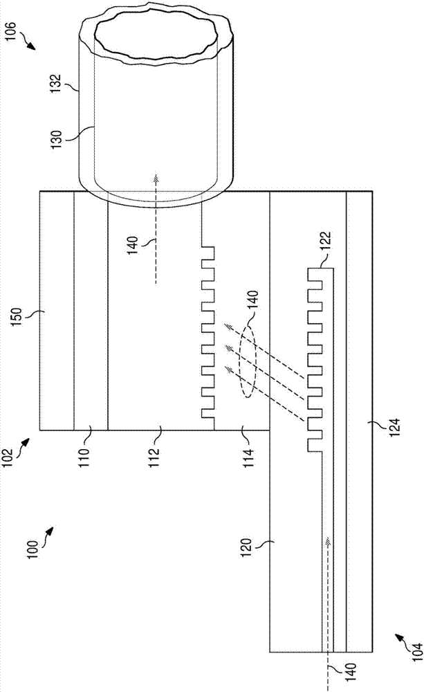
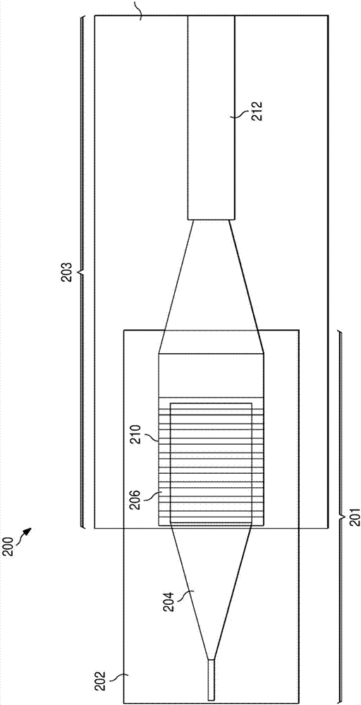
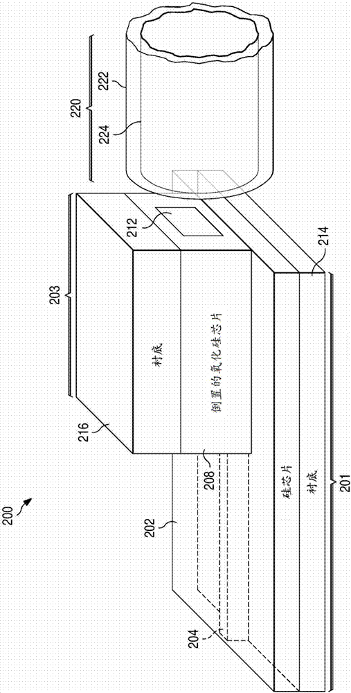
[0016] Silicon nanophotonic circuits exhibit high compactness as well as a high level of functional integration due to their high refractive index contrast based on SOI platforms. The waveguide cross-sections of silicon nanophotonic circuits are in the submicron range. In order to implement a silicon chip within a data optical transmission network, such circuitry must be connected to an optical fiber (or other optical transmission device), typically having a mode field dimension (MFD) of 10 microns. Such a mismatch between the silicon waveguide and the fiber...


PUM


Abstract

An optical coupler created by bonded photonic chip (104) coupler for Silicon-on-Insulator (SOI) chip-fiber (106) coupling is provided. An optical coupler for coupling a photonic chip (104) to an optical fiber (106) includes a photonic chip (104) comprising a nano-sized photonic waveguide (106), photonic optical diffraction surface grating (122), and a first cladding (120) covering the photonic waveguide (106) and the photonic grating (122); and an optical coupling chip (102) comprising a micron-sized coupling waveguide and a coupling optical diffraction surface grating (112) embedded in a first coupling cladding (114) and on a second coupling cladding (110), wherein the first coupling cladding (114) is connected to the first cladding (120), wherein the optical coupling chip (102) is configured to couple to light transmitted between the photonic chip (104) and an optical fiber (106).

Description

[0001] This application requires US Non-Provisional No. 14 / 515,211, entitled "Stacked Photonic Chip Coupler for SOI Chip-Fiber Coupling," filed October 15, 2014 The benefit of the application, the US non-provisional application is incorporated herein by reference. technical field [0002] The present invention relates to optical transmission systems and, in particular embodiments, to systems and apparatus for coupling photonic chips to optical fibers. Background technique [0003] Edge-coupling is a conventional method for realizing optical fiber-to-photonic chip coupling because edge-coupling can operate over a wide range of wavelengths and it is incompatible with mature packaging technologies such as silicon-on-silicon (silica-on-silicon) for larger photonic chips. on-silicon) technology. However, conventional edge coupling results in large optical losses (eg, fiber-to-SOI chips), which significantly affects the efficiency of photonic chips. Such optical losses are typic...

Claims


Application Information

Patent Timeline
Patent Type & Authority Applications(China)
IPC IPC(8): G02B6/30G02B6/34
CPCG02B6/1223G02B6/124G02B6/305G02B6/34G02B6/356G02B2006/12061G02B2006/12164H01L31/167
Inventor 蒋嘉
Owner HUAWEI TECH CO LTD
Why Eureka
Try Eureka