Standard reference for metrology and calibration method of electron-beam metrology system using the same

a metrology system and electron beam technology, applied in the field of electron beam metrology, can solve the problems of difficult development, limit the accuracy of diffraction angle measurement of grating using laser beam for calibrating purposes, and the exposure device whose laser beam source is altered to a shorter wavelength involves many problems, and achieves the effect of high accuracy, unprecedented size calibration, and easy differentiation

Inactive Publication Date: 2006-07-18
HITACHI HIGH-TECH CORP
View PDF4 Cites 22 Cited by
  • Summary
  • Abstract
  • Description
  • Claims
  • Application Information

AI Technical Summary

Benefits of technology

[0009]This makes possible, by arranging a pattern of or above a length for the same scanning range of an electron-beam or a probe, calibration permitting ready beam addressing. Further by arranging near this pattern a mark pattern whose shape is easily distinguishable from other patterns, recording of positional information measured with an electron-beam or a probe is made possible. Thus, by arranging a pattern permitting conventional diffraction angle measurement of grating by the use of a laser beam and a fine pattern matching the minimum machining dimensions of the latest semiconductor devices within the same member, a standard reference for metrology and calibration by which fineness and high accuracy are made compatible can be realized.
[0010]Further, by arranging patterns in the vertical direction and patterns in the lateral direction within the same member, unprecedented size calibration in both vertical and lateral directions can be realized at the same level of accuracy. By keeping the distance between these pattern units within 20 μm, calibration can be accomplished under the same optical conditions of the electron-beam metrology system, and accordingly a higher level of accuracy can be achieved.
[0011]Next will be described how this standard reference for metrology is fabricated. A conventional grating pattern and a fine pattern matching minimum machining dimensions of the latest semiconductor devices cannot be arranged within the same member by laser interferometer lithography using a conventional standard reference for metrology because of its limitation in resolution and in the freedom of pattern creation. In view of this problem, the invention uses electron-beam delineation excelling in resolution and unlimited in pattern shaping. For the fabrication of a highly accurate standard reference for metrology improved in uniformity in the specimen plane, an electron-beam cell projection exposure method by which the desired pattern is formed into a stencil mask and projected in a reduced size with an electron-beam for exposure is particularly effective. Thus, since a plurality of kinds of delineation patterns of grating in the vertical and lateral directions are all fabricated into stencil masks, accurately reproducible patterning is possible without dimensional variations from shot to shot by selecting the desired mask by beam deflection and exposing it to light repetitively. Combination of this patterning method and dry etching makes possible fine standard references for metrology suitable for use with an electron-beam metrology system of a scanning probe microscope. Formation of square apertures in stencil masks in advance would make possible variable shaped delineation with no limitation of the variety of patterns.
[0012]When a fine size is to be measured in calibrating an electron-beam metrology system with this standard reference, size calibration is accomplished with a proven fine grating pattern by using an electron-beam metrology system, a scanning probe microscope or a deep ultraviolet solid-state short-wavelength laser. Proper accomplishment of the calibration can be confirmed by measuring, after this calibration, the pitch size of a proven grating with a laser beam whose wavelength is absolutely guaranteed. The configuration is such that, if the measured size and the pitch size figured out from the diffraction angle surpass the reference, the electron-beam metrology system issues an alarm, and another fine pattern is used in that case. Thus, by calibrating the electron-beam metrology system again by using a fine pattern in another location than the previously used fine grating with reference to the mark pattern, the high level of calibration accuracy can be maintained.

Problems solved by technology

Exposure devices whose laser beam source is altered to a shorter wavelength involve many problems, and are difficult to develop.
Similarly, there is a limit to the accuracy of diffraction angle measurement of grating using a laser beam for the calibrating purpose, and such measuring is impossible at a minimum pitch below 200 nm approximately.
However, conventional standard references of dimensions cannot meet the requirements of the minimum machining dimensions of the latest semiconductor devices.
Therefore, it cannot be accurately specify the position of the grating pattern which was used in calibration with a pitch size proving device and a metrology system.
Where an electron-beam metrology system is used, consecutive use of any specific pattern would invite deterioration in calibration accuracy because the sticking of contamination ensuing from irradiation with a beam gives rise to dimensional variations in the specimen.

Method used


Image

  • Standard reference for metrology and calibration method of electron-beam metrology system using the same
  • Standard reference for metrology and calibration method of electron-beam metrology system using the same
  • Standard reference for metrology and calibration method of electron-beam metrology system using the same

Examples


Embodiment Construction

[0038]Preferred embodiments of the present invention will be described in detail below with reference to accompanying drawings.

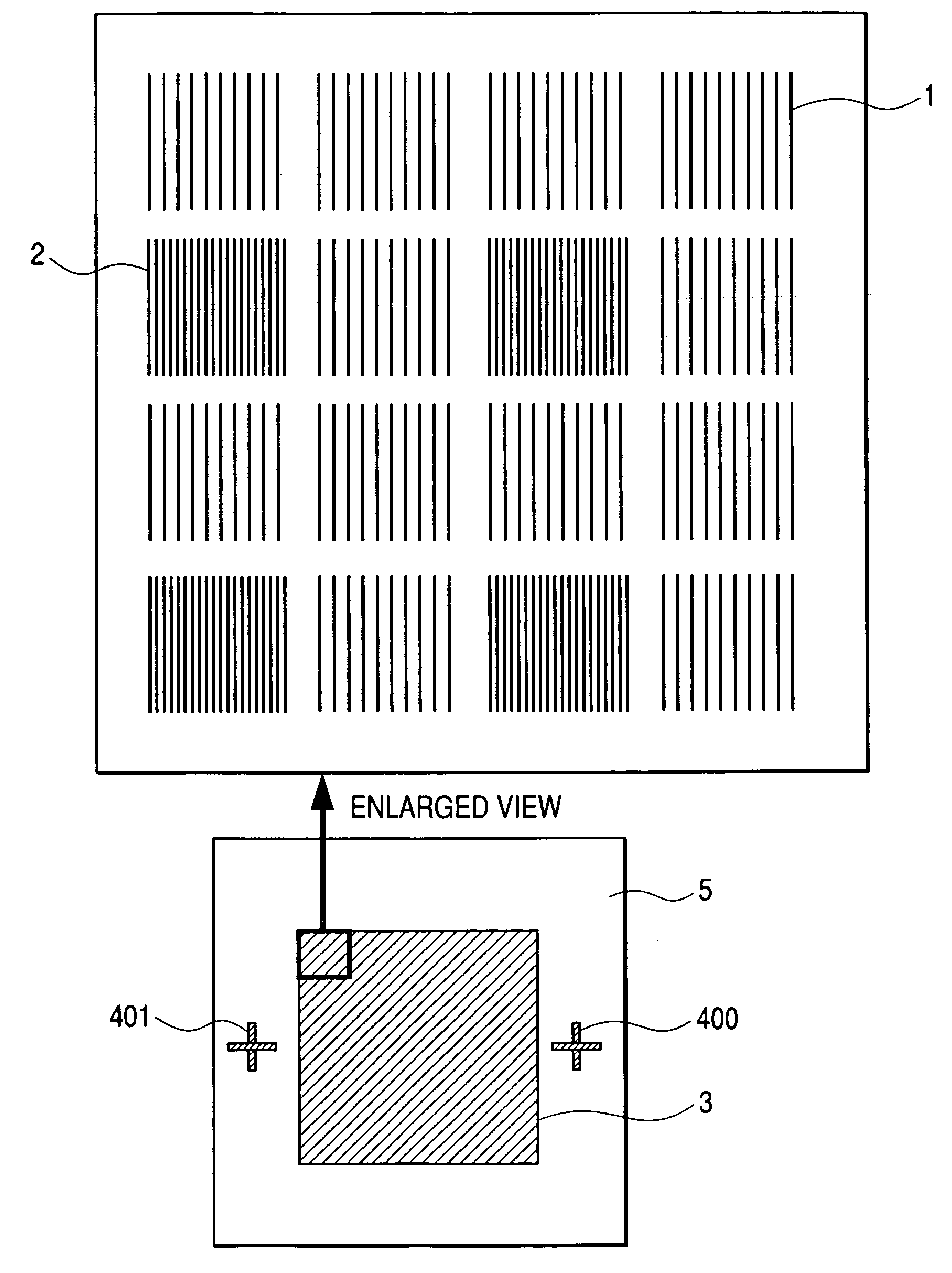
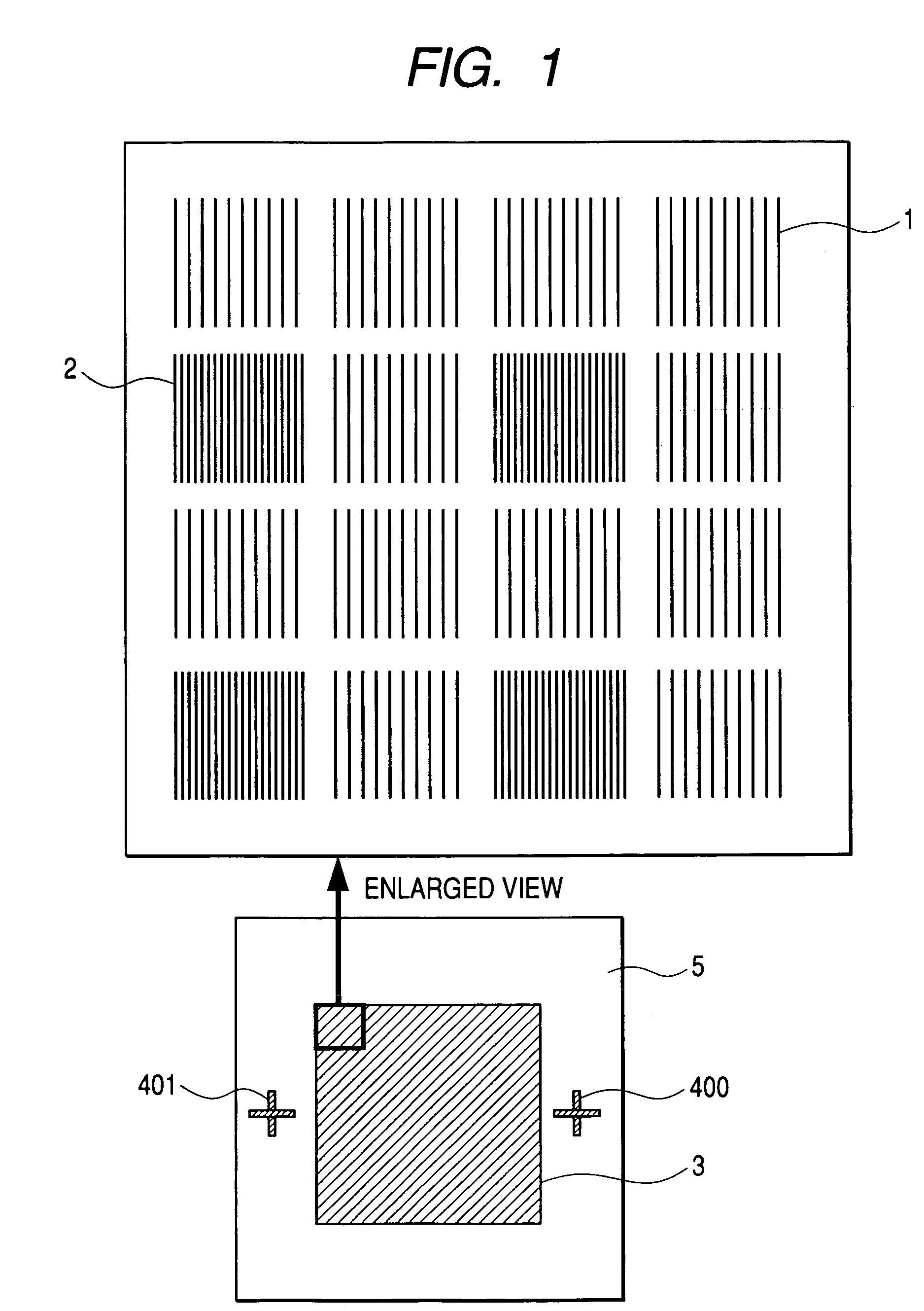
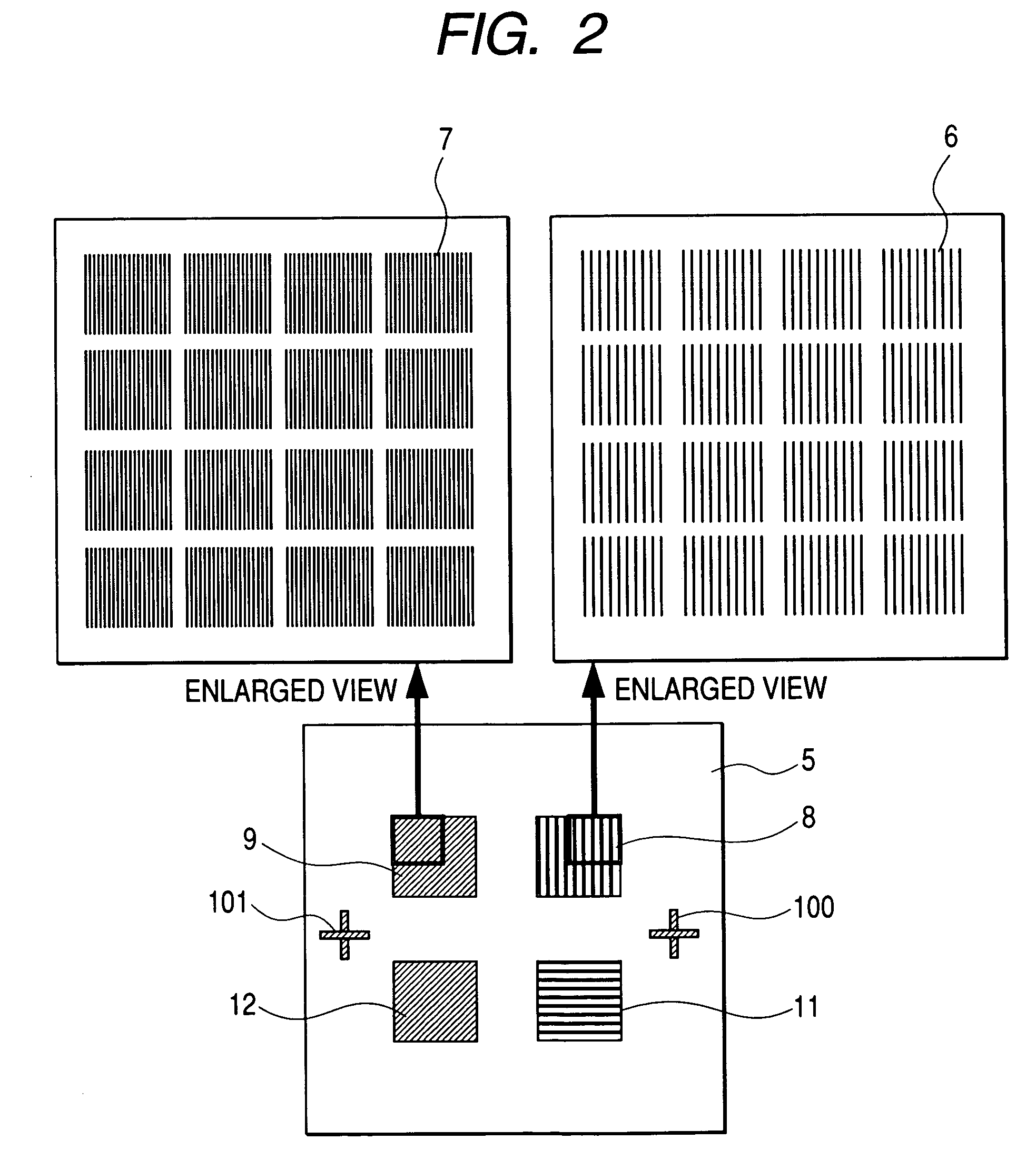
[0039]FIG. 1 through FIG. 5 show one example of standard reference for beam metrology according to the invention. FIG. 6 shows an example of standard reference for metrology for an electron-beam metrology system according to the prior art.

[0040]Conventionally, the trench pattern of unevenness on the semiconductor substrate of orientation (110) is prepared as a grating pattern 28 in a fixed direction by laser interferometer lithography and wet etching as shown in FIG. 6. The pitch of the grating pattern 28 is about 200 nm, and this value is obtained by diffraction angle measurement using a laser. The grating pattern 28 is formed all over a standard reference substrate 27 of 4 mm square. Calibration of an electron-beam metrology system using this reference substrate would involve the following problems.

[0041]The first problem concerns fineness. The latest semi...


PUM


Abstract

The present invention is to provide a standard reference for metrology having finer reference sizes and high-precision electron-beam metrology including the same. By using a standard reference member in which a grating unit pattern of a pitch size proven by an optical diffraction angle by using a laser beam whose wavelength is absolutely guaranteed and a plurality of patterns having a finer size than that (100 nm or less) over the same substrate, fineness and correctness of calibration are made verifiable on a regular basis, and by using an electron-beam collective exposure method for pattern fabrication, fabrication of this standard reference is made possible.

Description

CLAIM OF PRIORITY[0001]The present invention claims priority from Japanese application JP 2004-049218 filed on Feb. 25, 2004, the content of which is hereby incorporated by reference on to this application.BACKGROUND OF THE INVENTION[0002]The present invention relates to electron-beam metrology including a standard reference for metrology used in electron-beam metrology.[0003]Standard references for metrology for electron-beam metrology according to the prior art use a grating which is fabricated over a semiconductor substrate by laser interferometer lithography and anisotropic chemical etching. Their calibration is accomplished by measuring the diffraction angle of grating by the use of a laser beam whose absolute accuracy is guaranteed (see, for instance, Japanese Patent Application Laid-Open No. 7-71947).SUMMARY OF THE INVENTION[0004]The minimum possible dimensions for the standard references mentioned are determined by the resolution limit of laser interferometer lithography. Th...

Claims


Application Information

Patent Timeline
Patent Type & Authority Patents(United States)
IPC IPC(8): H01J37/304G01B15/00H01J37/28
CPCG01B15/00H01J37/28H01J2237/2826H01J2237/2814G01B21/042
Inventor NAKAYAMA, YOSHINORI
Owner HITACHI HIGH-TECH CORP
Why Eureka
Try Eureka