Method for depositing amorphous silicon membrane through PECVD (plasma enhanced chemical vapor deposition)

An amorphous silicon thin film and deposition technology, applied in the direction of gaseous chemical plating, coating, electrical components, etc., can solve problems such as the impact of product yield, and achieve the effect of reducing the generation of particles

Inactive Publication Date: 2017-08-22
SHANGHAI HUAHONG GRACE SEMICON MFG CORP
View PDF8 Cites 7 Cited by
  • Summary
  • Abstract
  • Description
  • Claims
  • Application Information

AI Technical Summary

Problems solved by technology

The disadvantage of the existing method of depositing amorphous silicon film by PECVD is that it is easy to form a lot of particles on the surface of the target wafer,

Method used


Image

  • Method for depositing amorphous silicon membrane through PECVD (plasma enhanced chemical vapor deposition)
  • Method for depositing amorphous silicon membrane through PECVD (plasma enhanced chemical vapor deposition)
  • Method for depositing amorphous silicon membrane through PECVD (plasma enhanced chemical vapor deposition)

Examples


Embodiment Construction

[0038] Because the method of the embodiment of the present invention is formed on the basis of breaking through the conventional thinking of those skilled in the art, the proposal of the technical problem of the present invention itself has creativity, so before introducing the method of the embodiment of the present invention in detail, first introduce the existing method:

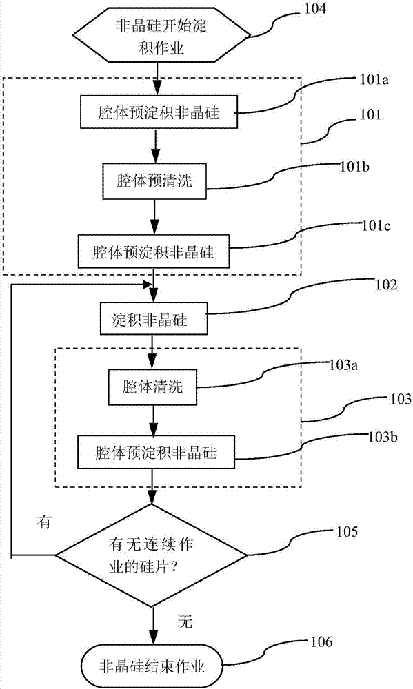
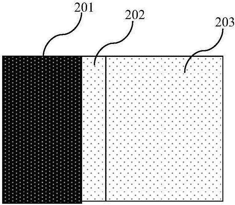
[0039] Such as figure 1 Shown is the flow chart of the method for depositing amorphous silicon thin film by existing PECVD; figure 2 Shown is the film structure diagram formed on the inner wall of the process chamber 201 in the existing method for depositing an amorphous silicon thin film by PECVD; the existing method for depositing an amorphous silicon thin film by PECVD includes steps:

[0040] The first step after starting the deposition of amorphous silicon, that is, step 1, is to perform an inter-batch pretreatment step, and the deposition of amorphous silicon starts at figure 1 Indicated by mark ...


PUM


Abstract

The invention discloses a method for depositing an amorphous silicon film by PECVD, which also includes a pretreatment step before the step of depositing the amorphous silicon film; the pretreatment step includes depositing a layer of intermediate The pre-deposition step of the dielectric layer; the adhesion and stress buffering capacity of the intermediate dielectric layer and the inner wall of the process chamber are greater than the adhesion and stress buffering capacity of the amorphous silicon film and the inner wall of the process chamber, and the intermediate dielectric layer and the amorphous silicon The adhesion and stress buffering capacity of the film are greater than the adhesion and stress buffering capacity of the amorphous silicon film and the inner wall of the process chamber, and the intermediate dielectric layer is used as a buffer layer between the inner wall of the process chamber and the amorphous silicon film on the inner wall and Prevent the amorphous silicon film on the inner wall of the process chamber from peeling off. The invention can reduce the generation of particles, improve the quality of the amorphous silicon film and improve the product yield.

Description

technical field [0001] The invention relates to a method for manufacturing a semiconductor integrated circuit, in particular to a method for depositing an amorphous silicon film by plasma enhanced chemical vapor deposition (PECVD). Background technique [0002] Amorphous silicon materials are widely used in various fields of semiconductors. When amorphous silicon is used in the post-metal process, it is necessary to use a lower temperature process to avoid the melting of metal lines. The PECVD deposition preparation method is almost the first choice. Program. The disadvantage of the existing method of depositing amorphous silicon film by PECVD is that it is easy to form a lot of particles on the surface of the target wafer, which is usually a silicon wafer. The film should be thinner, and there is obvious film separation at the edge of the pit, which will affect the yield of the product. Contents of the invention [0003] The technical problem to be solved by the present...

Claims


Application Information

Patent Timeline
IPC IPC(8): C23C16/24C23C16/02H01L21/02
CPCC23C16/24C23C16/0272H01L21/02532H01L21/02592H01L21/0262
Inventor 王剑敏
Owner SHANGHAI HUAHONG GRACE SEMICON MFG CORP
Why Eureka
Try Eureka