Sealing ring with esd protection

A technology of ESD protection and sealing ring, which is applied in the direction of semiconductor/solid-state device parts, semiconductor devices, electrical components, etc., and can solve problems such as not having ESD protection function

Active Publication Date: 2019-10-11
SHANGHAI HUAHONG GRACE SEMICON MFG CORP
View PDF6 Cites 0 Cited by
  • Summary
  • Abstract
  • Description
  • Claims
  • Application Information

AI Technical Summary

Problems solved by technology

[0005] therefore figure 1 The existing sealing ring shown has only a protection function against mechanical stress and does not have an ESD protection function

Method used


Image

  • Sealing ring with esd protection
  • Sealing ring with esd protection
  • Sealing ring with esd protection

Examples


no. 1 example

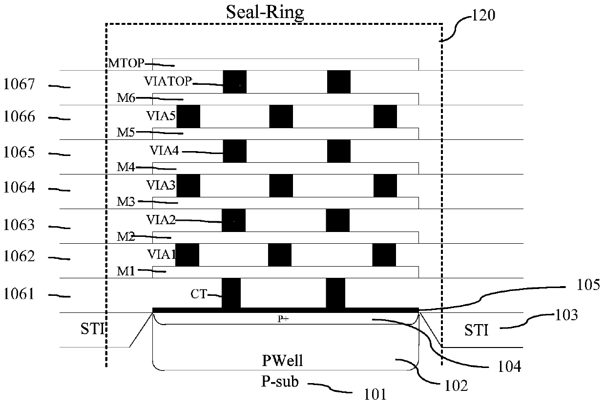
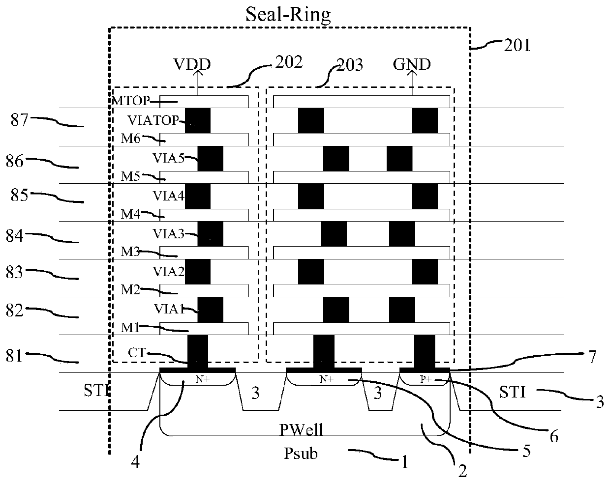
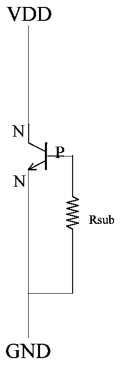
[0035] Such as Figure 2A Shown is a schematic diagram of a sealing ring with an ESD protection function according to the first embodiment of the present invention; Figure 2B yes Figure 2A The shown equivalent circuit diagram; the sealing ring with ESD protection function according to the first embodiment of the present invention includes: a substrate part structure formed in the semiconductor substrate 1 and a metal connection structure forming the top surface of the semiconductor substrate 1 . Figure 2A The middle semiconductor substrate 1 is a P-type semiconductor substrate, namely Psub. Preferably, the semiconductor substrate 1 is a silicon substrate.

[0036] A sealing ring with a stress protection function is formed by superposition of the substrate partial structure and the metal connection structure. Figure 2A The area of ​​the middle sealing ring is the area framed by the dotted box 201 .

[0037] The partial structure of the substrate includes:

[0038]The f...

no. 2 example

[0048] Such as Figure 3A Shown is a schematic diagram of a sealing ring with ESD protection function according to the second embodiment of the present invention; Figure 3B yes Figure 3A The shown equivalent circuit diagram; the difference between the second embodiment of the present invention and the first embodiment of the present invention is that in the second embodiment of the present invention:

[0049] The first conductivity type is N type, the second conductivity type is P type, and the bipolar transistor is a PNP transistor.

[0050] Figure 3A In , the area of ​​the sealing ring is the area framed by the dotted box 201a.

[0051] Figure 3A , so the above-mentioned first conductivity type well region is marked with mark 2a alone, and the first conductivity type well region 2a is an N-type well region (NWell); the first doped region is marked with 4a alone, and the second The doped region is marked with 5a alone, and the third doped region is marked with 6a alo...


PUM


Abstract

The invention discloses a sealing ring having an ESD protection function. The sealing ring comprises a substrate portion structure and a metal connection structure, wherein the substrate portion structure comprises a first conductive type well region, and first to third doping regions formed on a surface of the well region, wherein the first and second doping regions are both second conductive type heavy doping, the third doping region is first conductive type heavy doping, the first doping region, the first conductive type well region and the second doping region form a bipolar transistor, the metal connection structure comprises two electrode structures, the first electrode structure is electrically connected with the first doping region, the second electrode structure is electrically connected with the second and third doping regions, and a portion between a collector region and a base region of the bipolar transistor is made to be a reverse-biased structure through the voltage applied to the first and second electrode structures. The sealing ring is advantaged in that the ESD protection function is realized, an area of the sealing ring can be effectively utilized to realize an ESD protection structure, the area can be saved, and an integration level is improved.

Description

technical field [0001] The invention relates to a semiconductor integrated circuit, in particular to a sealing ring with ESD protection function. Background technique [0002] On the one hand, with the decrease of the feature size of semiconductor devices and the substantial improvement of chip integration, and the electromagnetic environment that semiconductor products need to adapt to is getting worse and worse, so the electrostatic discharge (ESD) protection design is important in improving the reliability and yield of products. appears to be very important. Usually, in order to achieve better ESD capability, the chip area that needs to be consumed is very considerable. [0003] On the other hand, the seal-ring structure is a very important part in the back-end process of semiconductor manufacturing. A seal ring is a stress protection ring around the periphery of an integrated circuit (IC). It protects the chip's internal circuitry from damage from the scribe line area...

Claims


Application Information

Patent Timeline
Patent Type & Authority Patents(China)
IPC IPC(8): H01L23/60H01L27/02
Inventor 吕斌
Owner SHANGHAI HUAHONG GRACE SEMICON MFG CORP
Why Eureka
Try Eureka