

Array substrate and preparation method thereof, display panel, and display equipment
A technology of an array substrate and a manufacturing method, which are applied in the fields of display devices, array substrates and manufacturing methods thereof, and display panels, can solve the problems of affecting yield, difficult to eliminate display Mura, disregarding the placement direction of excimer laser beams and thin film transistors, etc. , to achieve the effect of improving quality and yield and reducing visual defects
- Summary
- Abstract
- Description
- Claims
- Application Information
AI Technical Summary
Problems solved by technology
Method used
Image


Examples
Embodiment Construction
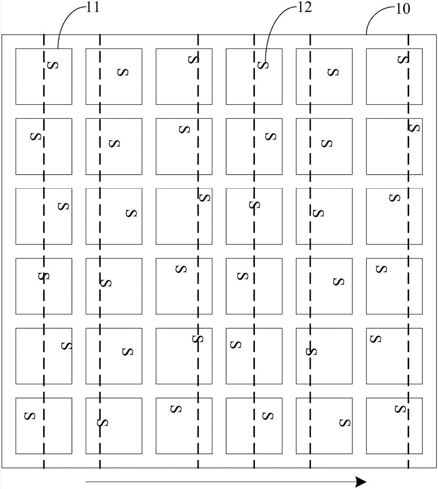
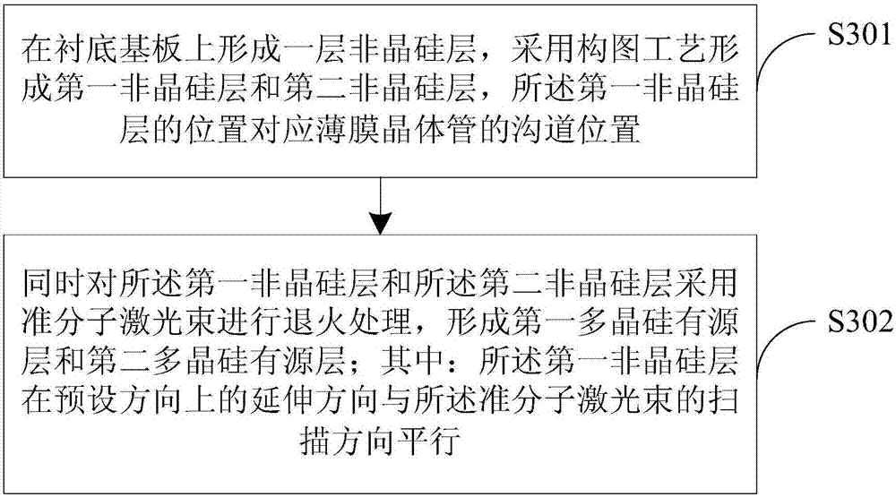
[0024] Embodiments of the present invention provide an array substrate and a manufacturing method thereof, a display panel, and a display device, which are used to reduce visual defects of display mura and improve the quality and yield of the array substrate.
[0025] In order to make the purpose, technical solutions and advantages of the present invention clearer, the present invention will be further described in detail below in conjunction with the accompanying drawings. Obviously, the described embodiments are only some of the embodiments of the present invention, rather than all of them. Based on the embodiments of the present invention, all other embodiments obtained by persons of ordinary skill in the art without making creative efforts belong to the protection scope of the present invention.
[0026] The array substrate provided by specific embodiments of the present invention will be described in detail below with reference to the accompanying drawings.
[0027] The t...
PUM
| Property | Measurement | Unit |
|---|---|---|
| Energy density | aaaaa | aaaaa |
Abstract
Description
Claims
Application Information