

Photo-thermal common-path interference module and method for measuring crystal defect
A common path, photothermal technology, applied in the direction of optical testing flaws/defects, testing crystals, color/spectral characteristics measurement, etc., can solve the lack of comparability, restricting the research and development of crystal materials, and the lack of uniform standards for crystal material measurement and other problems, to achieve the effect of large measurement range, good versatility and scalability, and high precision
- Summary
- Abstract
- Description
- Claims
- Application Information
AI Technical Summary
Problems solved by technology
Method used
Image

Examples
Embodiment 1
[0037] With laser crystal Nd:YVO 4 As an example, the three-dimensional distribution of crystal dynamic mesoscopic defects of the crystal is tested.
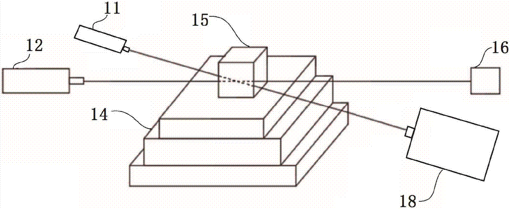
[0038] The structure of the photothermal common path interference module in this embodiment is as follows: figure 1 As shown, the photothermal common path interference module 1 includes a detection light source 11 , a pump light source 12 , a sample holder 14 , a laser power meter 16 and a wavefront detector 18 , and a sample 15 is placed on the sample holder 14 .
[0039] Specifically, the sample 15 is placed on a three-dimensionally movable sample holder 14, and the minimum moving step of the sample holder 14 is 10 μm.
[0040] The pump light source 12 adopts a 1064nm laser with a power of 30W, irradiates and passes through the sample 15, and then shoots to the laser power meter 16, and the laser power meter 16 records the optical power information. The laser beam emitted by the pump light source irradiates the sample with a...
Embodiment 2
[0044] With laser crystal Nd:YVO 4 As an example, the three-dimensional distribution of crystal dynamic mesoscopic defects of the crystal is tested.
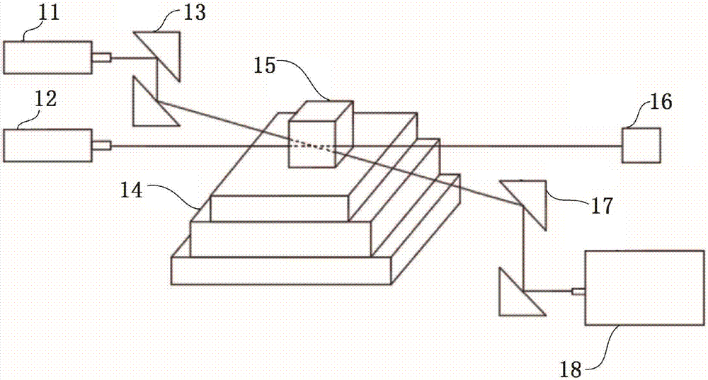
[0045] The structure of the photothermal common path interference module in this embodiment is as follows: figure 2 As shown, the photothermal common path interference module 1 includes a detection light source 11, a pump light source 12, a converging optical path 13, a sample holder 14, a laser power meter 16, a measuring optical path 17, and a wavefront detector 18. The sample 15 is placed on the sample Rack 14 above.
[0046] Specifically, the sample 15 is placed on a three-dimensionally movable sample holder 14, and the minimum moving step of the sample holder 14 is 10 μm.
[0047] The pump light source 12 adopts a 1064nm laser with a power of 10W, irradiates and passes through the sample 15, and then shoots to the laser power meter 16, and the laser power meter 16 records the optical power information. The laser beam em...
PUM
 Abstract
Description
Claims
Application Information