Production process of integrated surface-mounted light emitting device

A light-emitting device and production process technology, which is applied in the manufacture of electric solid-state devices, semiconductor devices, semiconductor/solid-state devices, etc., can solve the problems of inability to produce high-resolution display screens, welding yield of bracket pins, and technical difficulties in the production process, etc. problem, to achieve the effect of solving the difficulty of controlling the one-time pass rate, small size and high resolution

Active Publication Date: 2017-09-08
SHENZHEN ZIGUANG INTELLIGENT TECH CO LTD +1
View PDF3 Cites 5 Cited by
  • Summary
  • Abstract
  • Description
  • Claims
  • Application Information

AI Technical Summary

Problems solved by technology

[0003] There is only a single RGB chip in the light-emitting device made of this SMD package. Although the single lamp bead is easy to process, the four-corner or hexagonal bracket used in the package brings technical difficulties and reliability to the subsequent production process. Sexual hazards
When it is necessary to produce high-resolution display screens, the density of light-emitting points increases, and the light-emitting devices need to be patch-processed on the display circuit board. This SMD package structure has a large number of bracket pin welding yield problems, and cannot produce high-resolution screens. display screen

Method used


Image

  • Production process of integrated surface-mounted light emitting device
  • Production process of integrated surface-mounted light emitting device
  • Production process of integrated surface-mounted light emitting device

Examples


Embodiment Construction

[0025] The production process of the light emitting device proposed by the present invention includes the steps of encapsulation, cutting, binning, testing and the like.

[0026] Each step is explained in detail below:

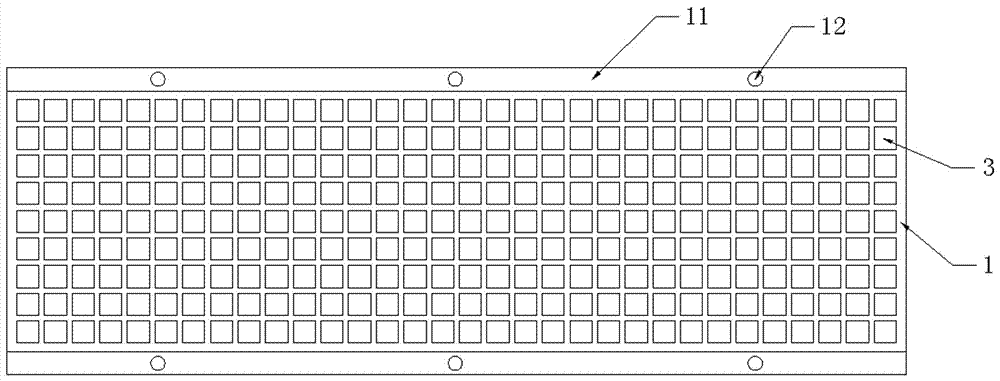
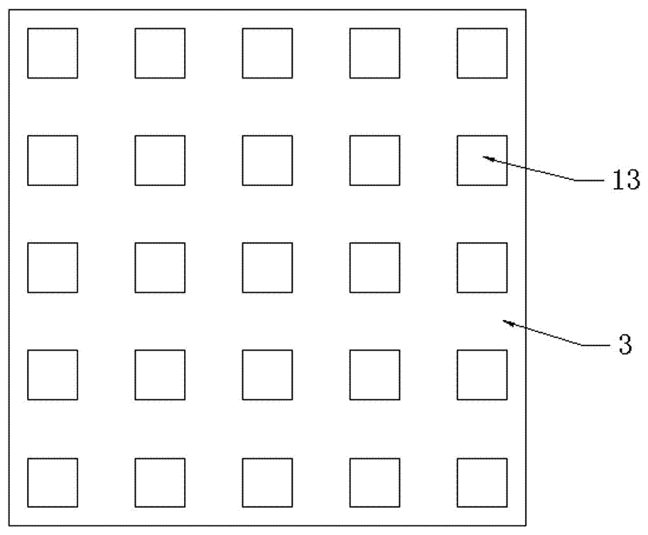
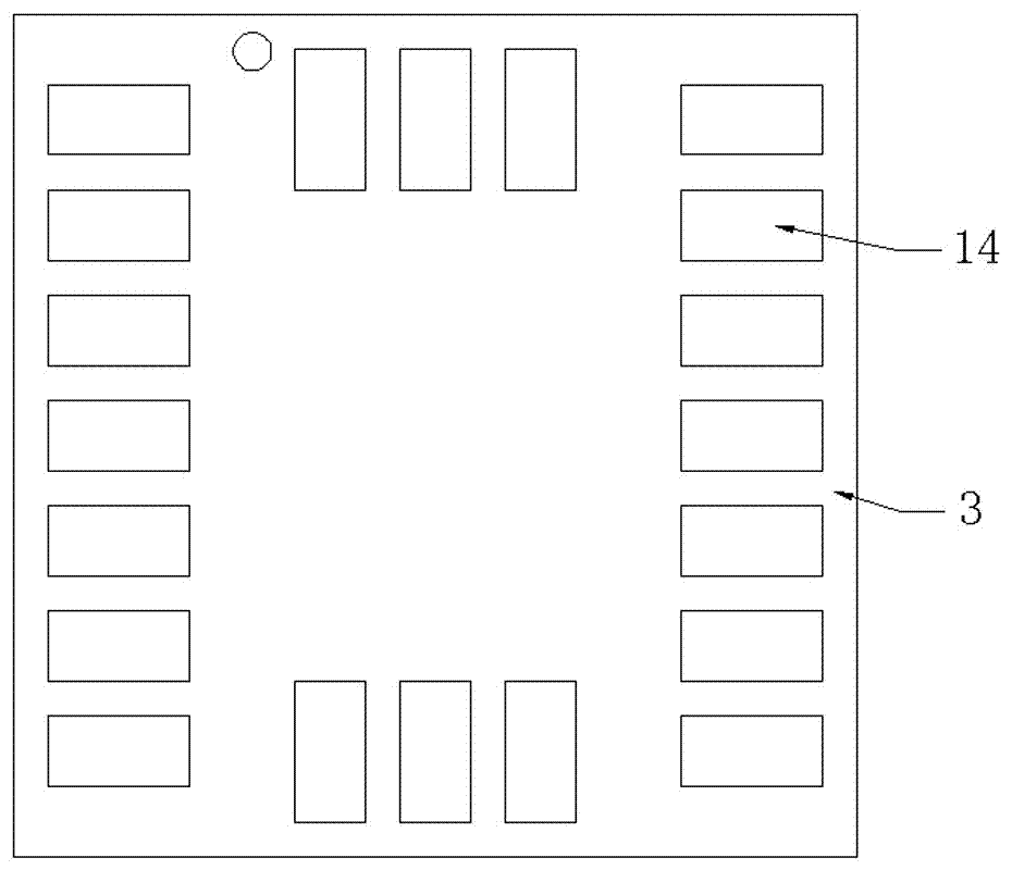
[0027] Step 1, such as figure 1 As shown, the substrate 1 is pre-imposed according to the needs. The upper and lower sides of the substrate 1 are provided with process edges 11, and the process edges 11 are provided with positioning holes 12 to facilitate subsequent processing on the substrate 1. Substrate 1 is a black double-sided circuit board or multi-layer circuit board. The material of substrate 1 is BT, carbon fiber or FR4. hole. Such as figure 2 , 3 As shown, the front of the substrate 1 is provided with several pads 13 for packaging LED chips, and the back of the substrate 1 is provided with several pads 14 for welding control pins.

[0028] Such as Figure 4 As shown, several light-emitting point groups are arranged and packaged on the front su...


PUM


Abstract

The invention discloses a production process of an integrated surface-mounted light emitting device. The production process comprises the following steps of 1, enabling a plurality of light emitting point groups to be arranged and packaged on the front surface of a substrate, wherein each light emitting point group comprises at least one red light LED chip, at least one green light LED chip and at least one blue light LED chip; and all LED chips are packaged on the substrate by adopting COB; 2, cutting the substrate into a plurality of independent light emitting devices, wherein one light emitting point group is arranged in each light emitting device; 3, lightening up the red light LED chips, the green light LED chips and the blue light LED chips in each light emitting device to test wavelength and luminance values, and allocating all light emitting devices with BIN according to the test data; and 4, testing forward voltage and reverse electric leakage of each light emitting device, and picking out the unqualified devices. The production process is simple, and the produced light emitting device is high in resolution.

Description

technical field [0001] The invention relates to the technical field of light-emitting components, in particular to a production process of an integrated surface-mounted light-emitting device. Background technique [0002] Most of the existing light-emitting display devices are packaged in SMD. In SMD packaging, the LED chip is fixed on the pad of the lamp bead bracket with conductive glue and insulating glue, and then the conductivity of the LED chip is soldered. After the functional test, use a ring Encapsulated with epoxy resin, and then split, cut and taped. [0003] There is only a single RGB chip in the light-emitting device made of this SMD package. Although the single lamp bead is easy to process, the four-corner or hexagonal bracket used in the package brings technical difficulties and reliability to the subsequent production process. sexual hazards. When it is necessary to produce high-resolution display screens, the density of light-emitting points increases, and...

Claims


Application Information

Patent Timeline
Patent Type & Authority Applications(China)
IPC IPC(8): H01L25/075H01L33/48H01L21/78G09F9/33
CPCG09F9/33H01L21/78H01L25/075H01L33/48
Inventor 朱希婕吴江辉
Owner SHENZHEN ZIGUANG INTELLIGENT TECH CO LTD
Why Eureka
Try Eureka