An absorbing optical modulator based on graphene coplanar traveling wave electrodes

A technology of traveling wave electrodes and optical modulators, which is applied in the field of optoelectronics, can solve the problems of limited RC constant, small modulation bandwidth, and large modulator volume, and achieve the effects of improving modulation efficiency, reducing size, and simple preparation process

Active Publication Date: 2019-05-10
UNIV OF ELECTRONICS SCI & TECH OF CHINA
View PDF1 Cites 1 Cited by
  • Summary
  • Abstract
  • Description
  • Claims
  • Application Information

AI Technical Summary

Problems solved by technology

[0006] Based on the above technical problems, the present invention provides a graphene-based coplanar traveling-wave electrode absorption optical modulator, which solves the problem that existing graphene-based optical modulators are limited by the large RC constant of the lumped electrode structure, which causes modulation The problem of relatively small bandwidth is based on the large volume of traditional optoelectronic material modulators and the current problem of strict alignment between the upper and lower electrodes in the graphene microstrip line traveling wave electrode structure.

Method used


Image

  • An absorbing optical modulator based on graphene coplanar traveling wave electrodes
  • An absorbing optical modulator based on graphene coplanar traveling wave electrodes
  • An absorbing optical modulator based on graphene coplanar traveling wave electrodes

Examples


specific Embodiment

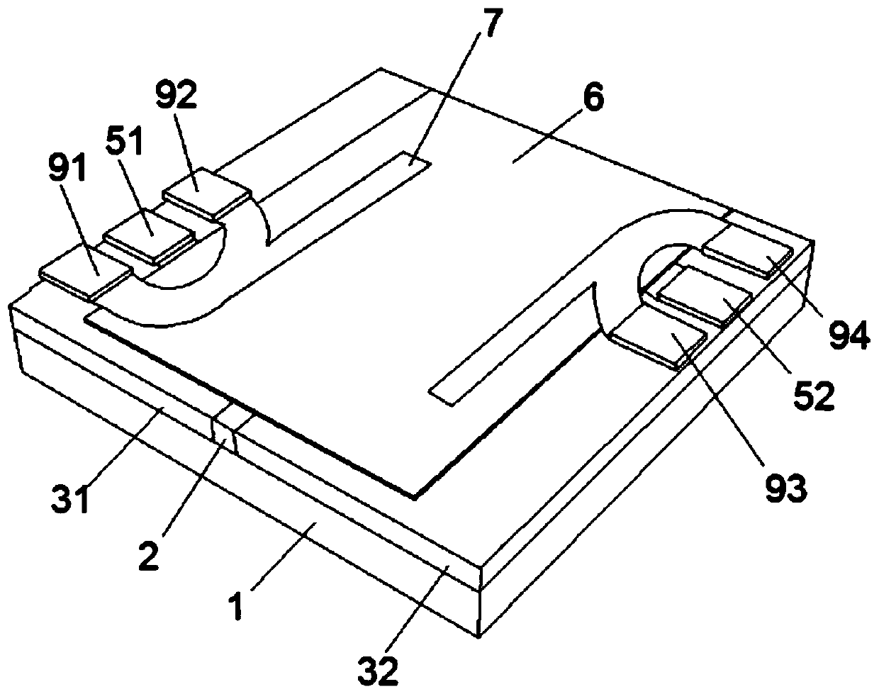
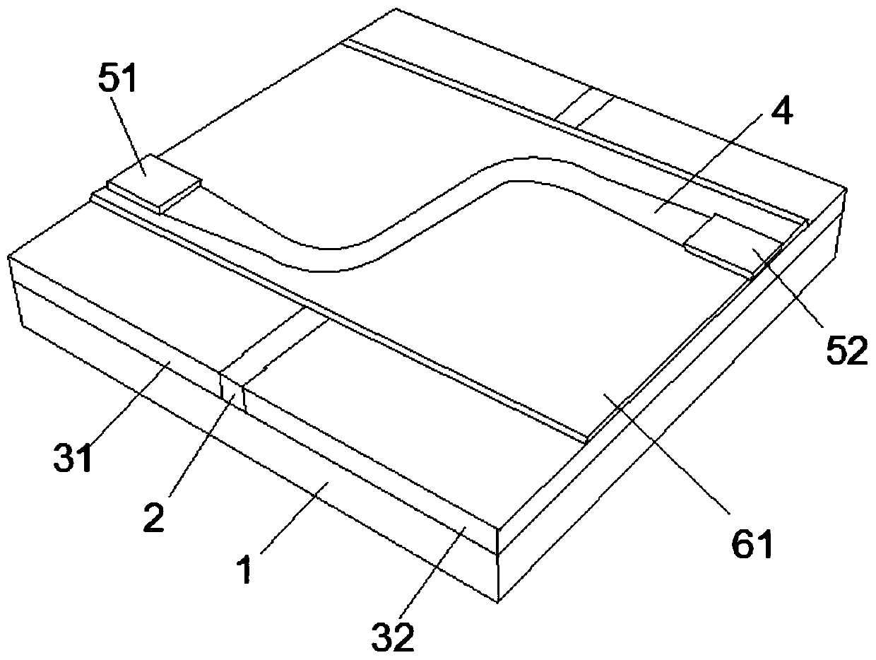
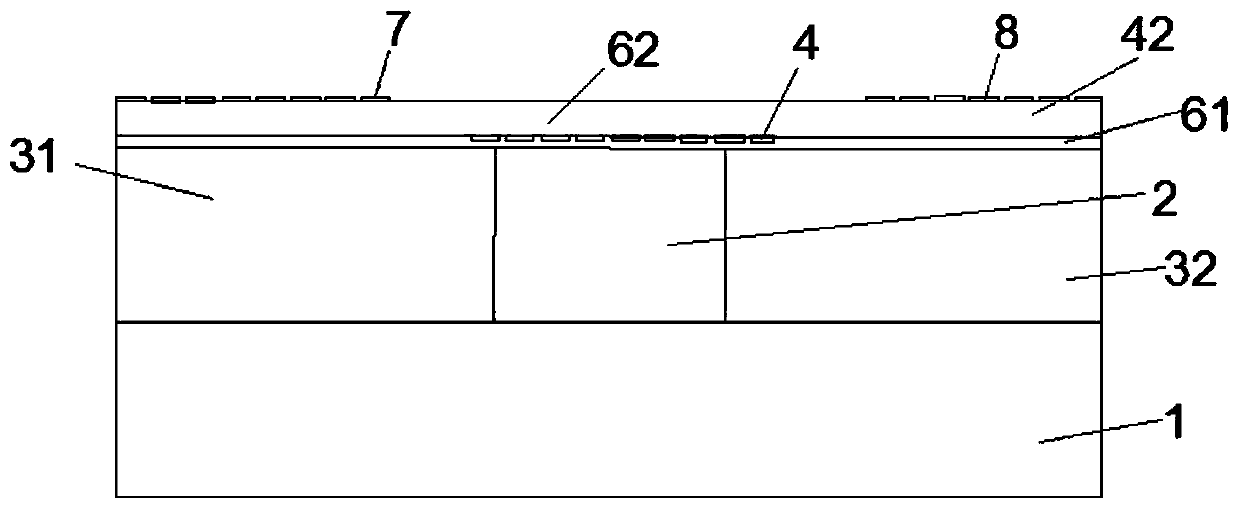
[0040] The schematic diagram of the structure of the graphene-based coplanar traveling-wave absorption optical modulator in this embodiment is as follows: figure 1 , figure 2 and image 3 shown. A light wave with a wavelength of 1.55 μm is used, and the light wave is connected from the strip optical waveguide 2 port. The height and width of the strip optical waveguide 2 are 220nm and 500nm respectively, and Si material is used; the first dielectric filling layer 31, the second dielectric filling layer 32 are all HSQ materials; the first dielectric isolation layer 61 and the second dielectric isolation layer 62 are respectively 5nm and 20nm thick SiN materials; the first graphene stripline 4, the second graphene stripline 7, and the third graphene stripline The material of the graphene stripline 8 is single-layer graphene, and the distance between each other is 5 μm; the width of the first graphene stripline 4 covered on the surface of the strip optical waveguide 2 is 5 μm; ...


PUM

PropertyMeasurementUnit
thicknessaaaaaaaaaa
thicknessaaaaaaaaaa
thicknessaaaaaaaaaa

Abstract

Belonging to the field of optoelectronic technology, a graphene-based coplanar traveling-wave electrode absorption type optical modulator is disclosed, including a substrate layer, a strip optical waveguide, a dielectric filling layer, a dielectric isolation layer, graphene striplines and electrodes, the A first dielectric isolation layer, a first graphene stripline, and a second dielectric isolation layer are sequentially arranged above the strip optical waveguide, and a second graphene stripline and a third graphene isolation layer are arranged on the second dielectric isolation layer. Stripline, the two ends of the first graphene stripline are respectively connected to the first electrode and the second electrode, one end of the second graphene stripline is connected to the first ground electrode and the second ground electrode, and the third One end of the graphene strip line is connected to the third ground electrode and the fourth ground electrode; this structure increases the bandwidth of the optical modulator, and at the same time, the optical modulator is compatible with the microwave probe, and the coplanar waveguide traveling wave electrode structure is adopted, and the preparation is relatively simple , to enhance the practicability of the device.

Description

technical field [0001] The invention relates to an optical modulator, in particular to an absorbing optical modulator based on a graphene coplanar traveling wave electrode, belonging to the technical field of optoelectronics. Background technique [0002] With the advent of the era of big data, data communication services are growing explosively, which makes people's demand for bandwidth higher and higher, which also determines the development of optical transmission systems in the direction of ultra-high speed, large capacity, and integration. Optical modulators and optical switches are the core devices in optical communication networks, and play an important role in the construction of optical communication networks. At present, optical modulators based on various mechanisms have been developed and prepared successively, and the current commercialized modulators are mainly based on lithium niobate materials and InP-based optical modulators. In recent years, Si-based optic...

Claims


Application Information

Patent Timeline
Patent Type & Authority Patents(China)
IPC IPC(8): G02F1/03G02F1/035
CPCG02F1/0316G02F1/035
Inventor 陆荣国叶胜威刘天良夏瑞杰陈德军张尚剑刘永
Owner UNIV OF ELECTRONICS SCI & TECH OF CHINA
Why Eureka
Try Eureka