Preparation method of in-situ electrified transmission electron microscope section sample of heterojunction film

A technology of transmission electron microscopy and heterojunction, which is applied in the direction of material analysis, measuring devices, and instruments using wave/particle radiation. It can solve the problems of inability to test the electrical properties of heterojunction thin films and difficult operation, and achieve a high success rate. , The sample preparation process is simple and the quality is good

Active Publication Date: 2017-09-15
GUANGXI UNIV
View PDF11 Cites 8 Cited by
  • Summary
  • Abstract
  • Description
  • Claims
  • Application Information

AI Technical Summary

Problems solved by technology

[0009] The purpose of the present invention is to provide a preparation method of in-situ energized transmission electron microscope cross-section samples of heterojunction films, so as to overcome the existing method of conducting transmission electron microscope experiments on cross-section samples of heterojunction films due to the need to use nano-conical The special in-situ electrified sample rod of the metal needle tip makes it impossible to test the electrical properties of the cross-sectional sample interface of the heterojunction film at the same time, and the operation is difficult.

Method used


Image

  • Preparation method of in-situ electrified transmission electron microscope section sample of heterojunction film
  • Preparation method of in-situ electrified transmission electron microscope section sample of heterojunction film
  • Preparation method of in-situ electrified transmission electron microscope section sample of heterojunction film

Examples


Embodiment Construction

[0025]The specific embodiments of the present invention will be described in detail below in conjunction with the accompanying drawings, but it should be understood that the protection scope of the present invention is not limited by the specific embodiments.

[0026] Unless expressly stated otherwise, throughout the specification and claims, the term "comprise" or variations thereof such as "includes" or "includes" and the like will be understood to include the stated elements or constituents, and not Other elements or other components are not excluded.

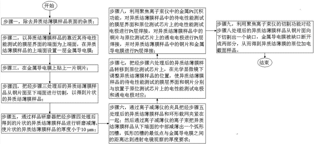
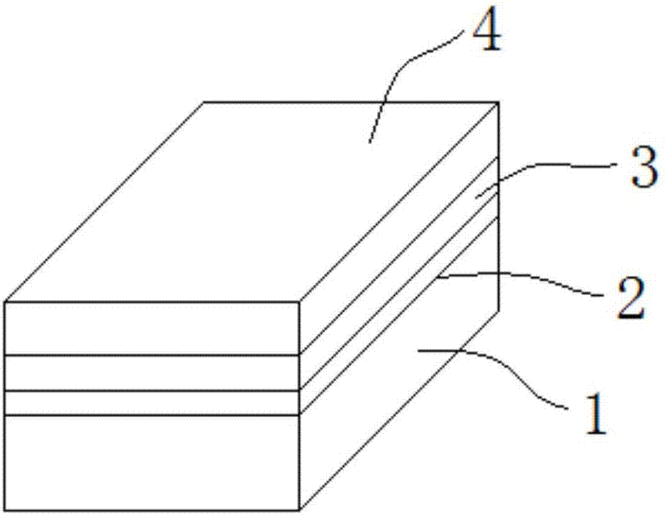
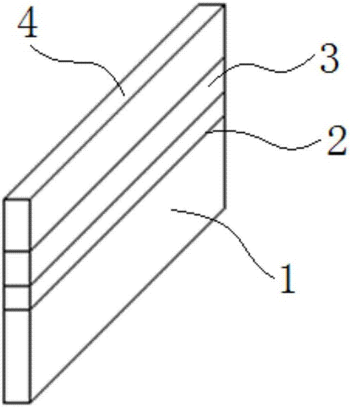
[0027] Figure 1 to Figure 4 A schematic diagram showing the structure of a method for preparing an in-situ energized transmission electron microscope section sample of a heterojunction film according to a preferred embodiment of the present invention, the preparation method of the in-situ energized transmission electron microscope section sample of the heterojunction film includes the following step:

[0028] Step 1, refe...


PUM

PropertyMeasurementUnit
thicknessaaaaaaaaaa

Abstract

The invention discloses a preparation method of an in-situ electrified transmission electron microscope section sample of heterojunction film; the preparation method comprises the steps of I, removing impurities on the surface of the heterojunction film sample; II, setting a layer of metal conductive film on the upper end face of the sample; III, attaching a copper sheet to the metal conductive film; IV, cutting the sample into a flaky sample; V, grinding to thin the flaky sample; VI, thinning the sample with an ionic thinner to obtain an arc recess; VII, transferring the sample to an in-situ test chip; VIII, using a focused ion beam instrument to weld a film layer interface and copper sheet, under electrical property test, of the sample respectively to an electrical property test electrode and power-on electrode of the in-situ test chip, and subjecting the copper sheet and metal conductive film to Pt layer welding; IX, cutting the sample to obtain a gap for breaking the metal conductive film. It is possible for the in-situ test chip to perform electrical property testing on the section sample of the heterojunction film, and operating is facilitated.

Description

technical field [0001] The invention relates to the field of preparation of section samples for in-situ electrification of a transmission electron microscope, in particular to a preparation method for an in-situ electrification transmission electron microscope section sample of a heterojunction thin film. Background technique [0002] The in-situ powered transmission electron microscopy experiment of heterojunction thin film samples is an effective means to understand the electrical regulation mechanism of functional information thin film materials. Usually the film thickness of the heterojunction thin film ranges from a few unit cells to tens of nanometers. Into the sample rod and realize the power supply and electrical property measurement function on the specific film layer. [0003] As far as the preparation of cross-sectional samples of heterojunction thin films for TEM is concerned, ion thinning technique (PIPS) and focused ion beam (FIB) cutting are two existing meth...

Claims


Application Information

Patent Timeline
Patent Type & Authority Applications(China)
IPC IPC(8): G01N23/22
CPCG01N23/2202
Inventor 王双宝沈培康田植群尹诗斌朱莉安·D·V·凯潘智毅
Owner GUANGXI UNIV
Why Eureka
Try Eureka