Cellular layout, cellular structure and manufacturing method of silicon carbide junction barrier schottky diode

A production method and technology of silicon carbide, applied in the direction of electrical components, semiconductor/solid-state device manufacturing, circuits, etc., can solve the problems of waste, device damage, easy burning, etc., and achieve the effect of not being easily damaged

Inactive Publication Date: 2017-09-15
YANGZHOU YANGJIE ELECTRONIC TECH CO LTD
View PDF4 Cites 13 Cited by
  • Summary
  • Abstract
  • Description
  • Claims
  • Application Information

AI Technical Summary

Problems solved by technology

When the junction barrier Schottky diode is subjected to directional energy, the electric field in the small-angle P-doped region is more concentrated (such as Figure 3-2 as shown, Figure 3-1 It is a schematic diagram of the electric field under normal conditions), the reverse bearing capacity is limited, and it is easy to burn out and cause damage to the entire device, thereby affecting the stable operation of the device, causing waste and potential safety hazards

Method used


Image

  • Cellular layout, cellular structure and manufacturing method of silicon carbide junction barrier schottky diode
  • Cellular layout, cellular structure and manufacturing method of silicon carbide junction barrier schottky diode
  • Cellular layout, cellular structure and manufacturing method of silicon carbide junction barrier schottky diode

Examples


Embodiment Construction

[0027] The present invention will be further described below in conjunction with specific drawings.

[0028] The following will clearly and completely describe the technical solutions in the embodiments of the present invention with reference to the accompanying drawings in the embodiments of the present invention. Obviously, the described embodiments are only some, not all, embodiments of the present invention. Based on the embodiments of the present invention, all other embodiments obtained by persons of ordinary skill in the art without creative efforts fall within the protection scope of the present invention.

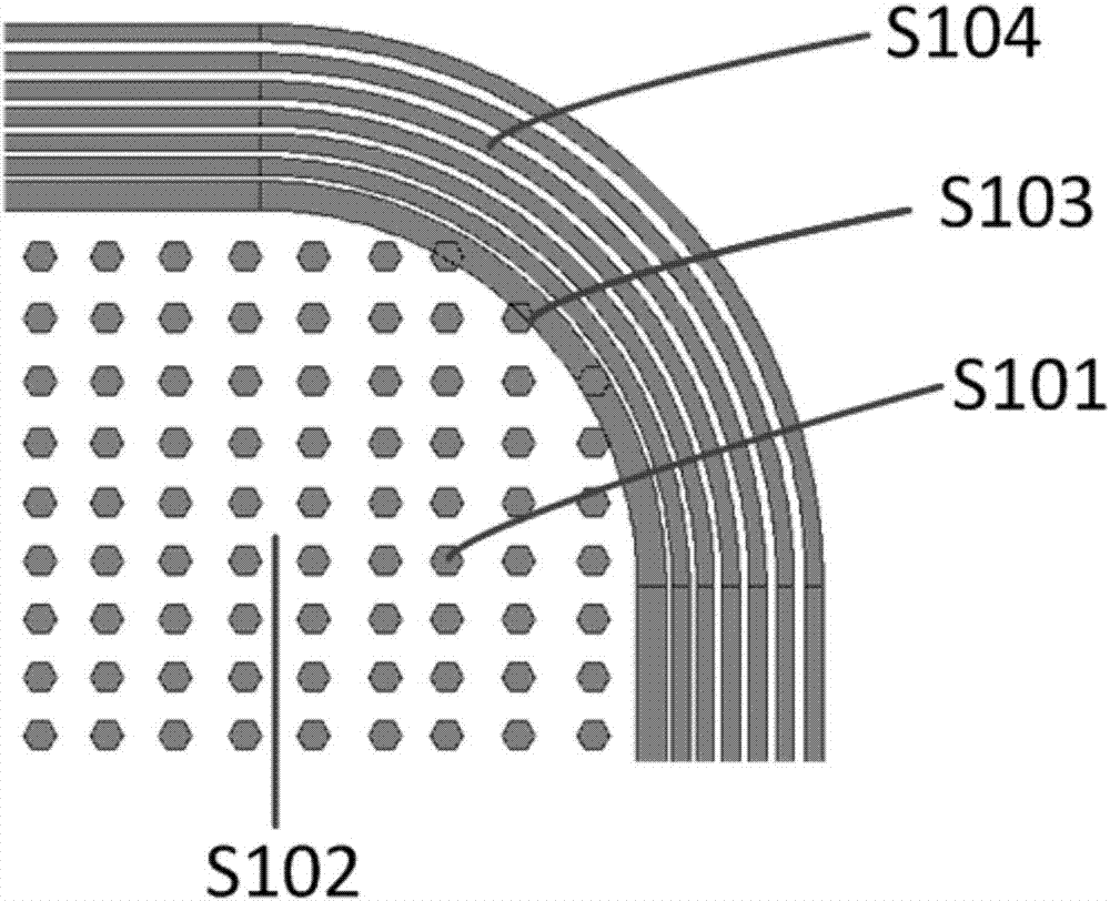
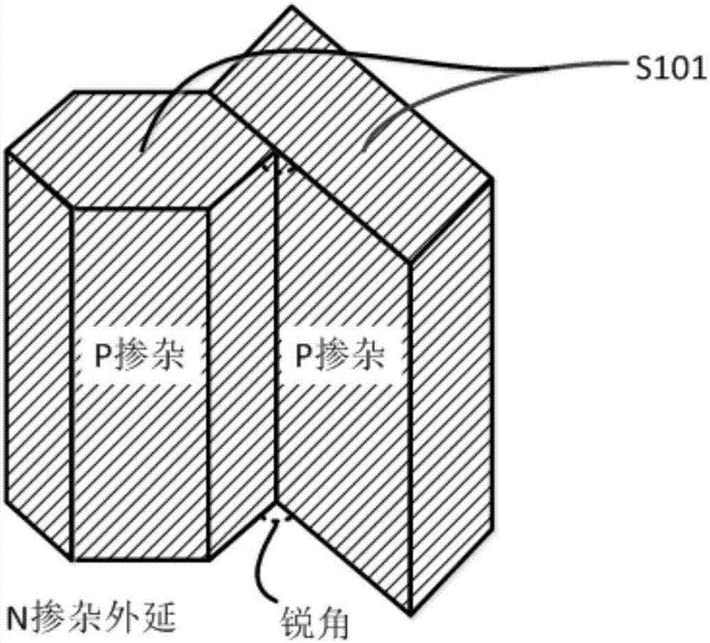
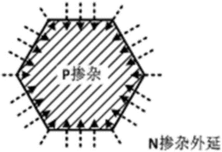
[0029] Such as Figure 4 As shown, it is the cell layout of the present invention, which is used to make the cell structure of the silicon carbide junction barrier Schottky diode. In this embodiment, the cellular layout of the present invention includes a cellular region 101, a transition region 103 surrounding the cellular region 101, a terminal region 104 on the...


PUM

PropertyMeasurementUnit
thicknessaaaaaaaaaa
angleaaaaaaaaaa

Abstract

The invention relates to a cellular layout, a cellular structure and a manufacturing method of a silicon carbide junction barrier schottky diode. The silicon carbide junction barrier schottky diode comprises a silicon carbide substrate, an epitaxial layer on the substrate and a P-doped region formed on the epitaxial layer in an injection manner; and the P-doped region is formed by circular/polygonal cells and strip-shaped cells in a mixed manner. By virtue of the circular/polygonal cells, the schottky contact area occupation ratio is improved, and the forward current density of a device is improved; by virtue of the strip-shaped cells, sharps formed by the cells in the corner positions and annular transitional regions can be eliminated, the reverse voltage withstand performance of the device is improved, and the device is not burn down easily; and in addition, the safety performance of the device is improved, the forward current density of the device is improved, and cost is lowered.

Description

technical field [0001] The invention relates to a cell layout, a cell structure and a method for manufacturing a silicon carbide junction barrier Schottky diode, belonging to the technical field of semiconductors. Background technique [0002] Silicon carbide material has unique advantages such as large bandgap width, high critical breakdown electric field, and high thermal conductivity. It is an ideal semiconductor material for making high withstand voltage, high power, and high temperature resistant devices. Junction barrier Schottky diodes made of silicon carbide materials have the advantages of high withstand voltage, high current, and fast recovery, and have broad application prospects in military and civil affairs. [0003] In traditional technology, in the layout structure design of silicon carbide junction barrier Schottky diodes, the cell structure has strip, square and polygonal structures. The strip cell structure improves the reverse withstand voltage capability...

Claims


Application Information

Patent Timeline
Patent Type & Authority Applications(China)
IPC IPC(8): H01L29/872H01L21/329H01L29/06
CPCH01L29/0661H01L29/6606H01L29/872H01L29/0619H01L29/0692
Inventor 唐亚超何钧赵群徐俊王陆委王毅
Owner YANGZHOU YANGJIE ELECTRONIC TECH CO LTD
Why Eureka
Try Eureka