
A high-precision array analog-to-digital converter for cmos image sensors

An analog-to-digital converter and image sensor technology, which is applied in the directions of image communication, color TV components, TV system components, etc. Limiting the design of successive approximation analog-to-digital converters and other issues to achieve the effect of reducing dynamic performance degradation and saving capacitor arrays

Inactive Publication Date: 2020-04-17
JILIN UNIV
View PDF7 Cites 0 Cited by
  • Summary
  • Abstract
  • Description
  • Claims
  • Application Information

AI Technical Summary

Problems solved by technology

The successive approximation analog-to-digital converter (SAR ADC) usually adopts a charge redistribution structure. Since the total unit capacitance of the capacitive successive approximation analog-to-digital converter is exponentially related to the accuracy of the analog-to-digital converter (ADC), for higher For a successive approximation analog-to-digital converter (SAR ADC) with high precision, the total amount of capacitance and chip area will increase sharply, and the dynamic power consumption consumed when switching capacitors will also increase accordingly.
[0007] Therefore, for high-precision capacitive successive approximation analog-to-digital converters, it is usually necessary to use a large capacitor, which results in: large charge and discharge power consumption, large area required for making chips, and increased economic costs.
At the same time, due to the improvement of the accuracy of the analog-to-digital converter, capacitance mismatch, comparator comparison error, etc. have a greater impact on the analog-to-digital converter, which limits the design of the successive approximation analog-to-digital converter

Method used


Image

  • A high-precision array analog-to-digital converter for cmos image sensors
  • A high-precision array analog-to-digital converter for cmos image sensors
  • A high-precision array analog-to-digital converter for cmos image sensors

Examples


Embodiment Construction

[0030] The present invention will be further described below in conjunction with the accompanying drawings.

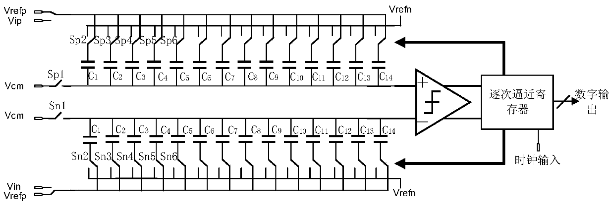
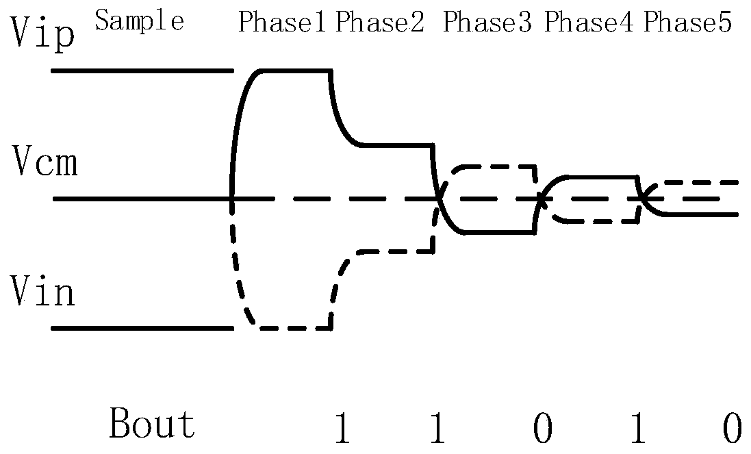
[0031] Such as figure 2 As shown, the SAR ADC adopts a fully differential structure. Take one end as an example: During the sampling phase, the bottom plate of the capacitor is connected to Vip, and the top plate of the capacitor is connected to the common-mode voltage Vcm. Next, the top plate of the highest bit capacitor is converted from the common mode voltage Vcm to Vrefp, and the top plate of other bit capacitors is switched to connect to Vrefn. At this time, the comparator performs the first comparison and outputs the comparison result. If Vip is greater than Vin, the highest bit (MSB for short) value B1 is binary 1, otherwise, it is 0. At the same time, the top plate of the highest bit capacitor is switched to Vrefn. Then the top plate of the sub-high capacitor is connected to Vrefp, and the comparator performs the second comparison and outputs the comparison...


PUM


Abstract

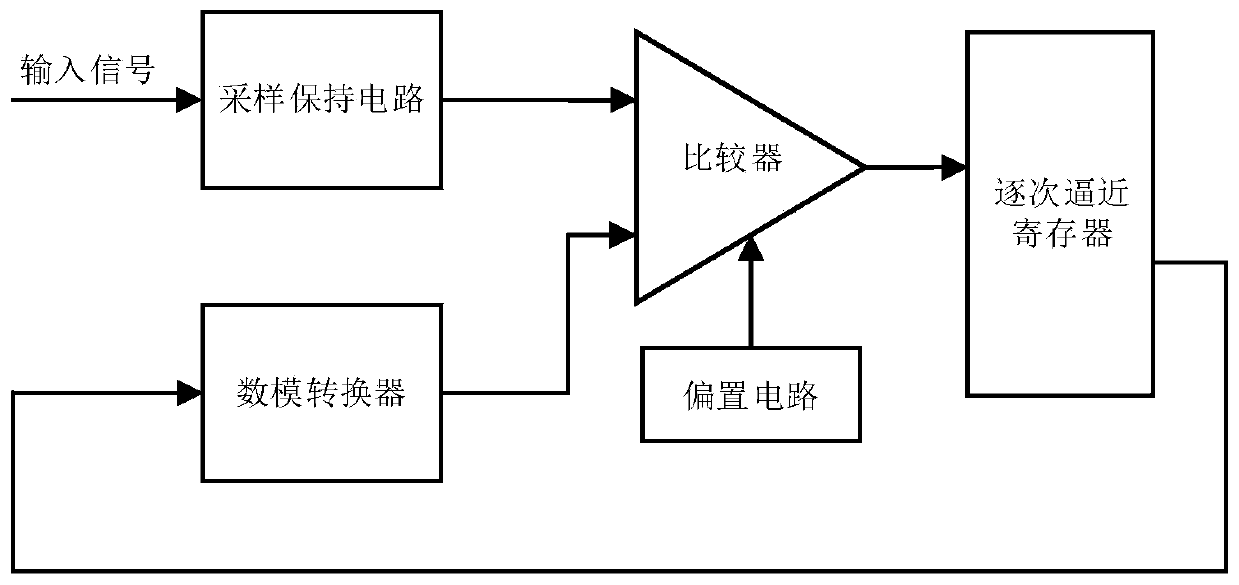
The invention discloses a high-precision array analog-to-digital converter applied to a CMOS image sensor, which belongs to the technical field of analog circuit design and includes a sample-and-hold circuit, a comparator, a digital-to-analog converter, a successive approximation register, and a digital error correction circuit; The analog-to-digital converter described above adopts a fully differential structure. The input signal is output to the top board of the capacitor array through a sample-and-hold circuit and connected to the input terminal of the comparator. The output terminal of the comparator is connected to the successive approximation register. The successive approximation register controls the capacitor array according to the result of the comparator And store it, and output it to the digital error correction circuit to get the final binary output. In the present invention, the capacitor array is divided into three capacitor arrays, wherein each capacitor array adopts a non-binary redundant capacitor architecture design, and the incomplete establishment of the circuit, the jitter and noise of the reference voltage and the metastable state of the dynamic comparator are caused There is a degree of tolerance for comparison errors. A dynamic comparator is also used without quiescent current, which effectively reduces the power consumption of the overall circuit.

Description

technical field [0001] The invention belongs to the technical field of analog circuit design, and in particular relates to an array successive approximation analog-to-digital converter applied to a CMOS image sensor. Background technique [0002] With the rapid development of CMOS technology, various systems have higher and higher requirements for analog-to-digital converters. The current development trend of ADC mainly has the following two directions: [0003] 1. Develop in the direction of low power consumption and small area [0004] With the increasing scale of integrated circuits, power consumption has become an important indicator for comparing chips with similar performance. Facing the development of CMOS technology, the technology of CMOS has been continuously improved, from a few um to the current tens of nanometers, and the power supply voltage required by each module is also continuously reduced. Continuously improve power consumption through power sleep mode,...

Claims


Application Information

Patent Timeline
Patent Type & Authority Patents(China)
IPC IPC(8): H04N5/3745H04N5/378
CPCH04N25/772H04N25/75
Inventor 常玉春杨姝刘明杭慕雨松徐弘基李亮孙睿智臧范军王仁广张东旭
Owner JILIN UNIV
Learn More