Process method for printing soldering paste bodies on circuit board in three-dimensional (3D) manner

A printed circuit board and 3D printing technology, which is applied in the direction of assembling printed circuits with electrical components, can solve the problems of inaccurate control of the shape of solder paste, easy clogging, poor shape accuracy of solder paste body, etc.

Active Publication Date: 2017-09-19
成都联创鸿发科技有限公司
View PDF3 Cites 9 Cited by
  • Summary
  • Abstract
  • Description
  • Claims
  • Application Information

AI Technical Summary

Problems solved by technology

[0005] Since the solder paste printing and coating method uses air pressure on the finished solder paste, the solder paste is sprayed on the printed board, and each pad is arranged in a matrix of dot-shaped solder paste to form the final solder paste body, although the solder paste The amount can be controlled according to the size of the pad, but since the solder paste body is composed of multiple dot-shaped solder paste, its shape is uncontrollable, and the poor shape accuracy of the solder paste body makes it easy to short circuit when soldering small packaged devices
In addition, in order to obtain good precision by spraying solder paste, we have to use nozzles with small calibers. The smaller the caliber, the easier it is to clog
Although the solder paste printing does not require the solder paste stencil in the stencil coating method, in this coating method, each solder paste body needs to be sprayed with dot-shaped solder paste multiple times to complete, resulting in poor solder paste coating. The efficiency is very low, the most important thing is that the shape of the solder paste cannot be precisely controlled

Method used


Image

  • Process method for printing soldering paste bodies on circuit board in three-dimensional (3D) manner
  • Process method for printing soldering paste bodies on circuit board in three-dimensional (3D) manner
  • Process method for printing soldering paste bodies on circuit board in three-dimensional (3D) manner

Examples


Embodiment Construction

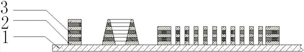
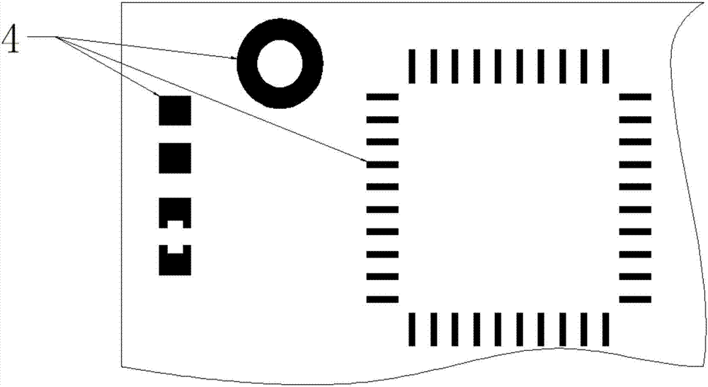
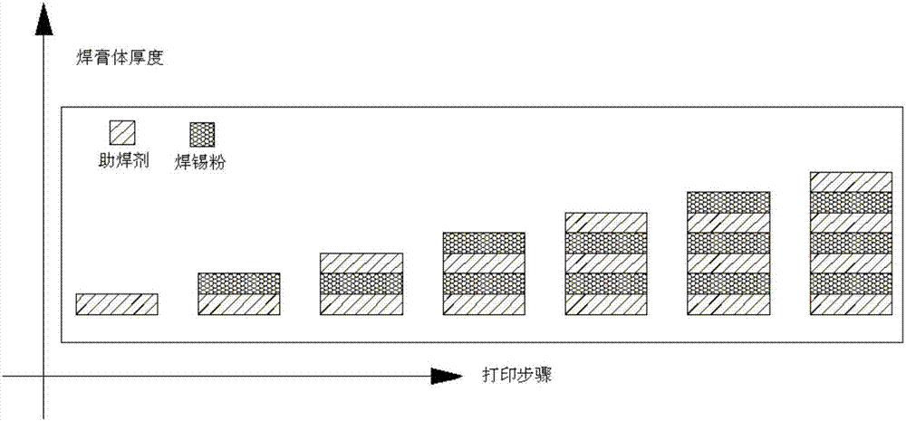
[0019] refer to Figure 1 ~ Figure 4 . According to the present invention, at the component pad position on the printed circuit board, the thickness of each layer of flux in the solder paste body and the thickness of each layer of solder layer are controlled by different 3D printing heads, 3D printed layer files and printing programs. The thickness of the powder, first print a layer of flux consistent with the shape of the pad on all pads of the printed board as the solder powder fixing medium, then print a layer of solder powder on the flux at these positions, and print layer by layer After completing an independent solder paste body, the next solder paste body is printed, and the flux 2 and solder powder 3 printed layer by layer are mixed, and the solder paste body 4 is formed in real time during the printing process, so that the layer-by-layer printing is alternately printed one by one. Layers of flux and solder powder are alternately printed to form the required solder pa...


PUM


Abstract

The invention provides a process method for printing soldering paste bodies on a circuit board in a three-dimensional (3D) manner. The process method is a process method capable of accurately printing soldering paste bodies in a three-dimensional (3D) manner. With the process method adopted, the shapes of the soldering paste bodies are controllable, the coating efficiency of soldering paste is high, and different thickness and different shapes can be realized. According to the technical schemes of the invention, the process method is implemented through following manners: a layer of flux of which the shape conforms to the shape of a pad is printed so as to be adopted as a solder powder fixing medium; a layer of solder powder is printed on the flux at a position where the pad is located; after one independent soldering paste body is obtained through layer-by-layer printing, a next soldering paste body is printed; flux layers and solder powder layers which are printed layer by layer are mixed, so that the soldering paste bodies can be formed in real time in a printing process; the flux layers and solder powder layers are printed alternately so as to form required soldering paste bodies; flux is printed at the last layer, so that the 3D printing of the soldering paste is terminated; and flux and solder powder multi-layer liquid naturally compounded soldering paste body layout distribution of different thicknesses and different shapes can be formed on the same printed circuit board.

Description

technical field [0001] The invention relates to the application of solder paste coating in the assembly process of printed boards in electronic products, which is used to realize accurate 3D printing of solder paste bodies with different thicknesses and shapes in the same printed board without missing a printing template. Background technique [0002] Nowadays, electronic assembly technology has generally adopted electronic assembly technology SMT. In a broad sense, the new generation of electronic assembly technology, that is, surface mount technology SMT, includes surface mount components SMC, surface mount devices SMD, surface mount printed circuit boards SMB, ordinary mixed printed circuit boards PCB, dispensing, coating, etc. Technical content such as paste, surface mount equipment, component pick and place system, soldering and online testing, is a collective term for a complete set of technological processes. In the SMT production process, the use of metal stencils t...

Claims


Application Information

Patent Timeline
Patent Type & Authority Applications(China)
IPC IPC(8): H05K3/34
Inventor 李颖岳婷莉阎红梅
Owner 成都联创鸿发科技有限公司
Why Eureka
Try Eureka