Fabrication method of array substrate mother board, array substrate mother board and detection method
A technology of an array substrate and a detection method, which is applied to the coating equipment, measuring device, and exposure device of the photoengraving process, etc., can solve the problems of low efficiency and low precision, and achieve high measurement efficiency, small measurement deviation, and measurement high precision effect
- Summary
- Abstract
- Description
- Claims
- Application Information
AI Technical Summary
Problems solved by technology
Method used
Image

Examples
Embodiment 1
[0044] Embodiment 1 of the present invention provides a method for preparing an array substrate mother board, combining Figure 1 to Figure 4 As shown, the preparation method of the array substrate motherboard includes the following steps:
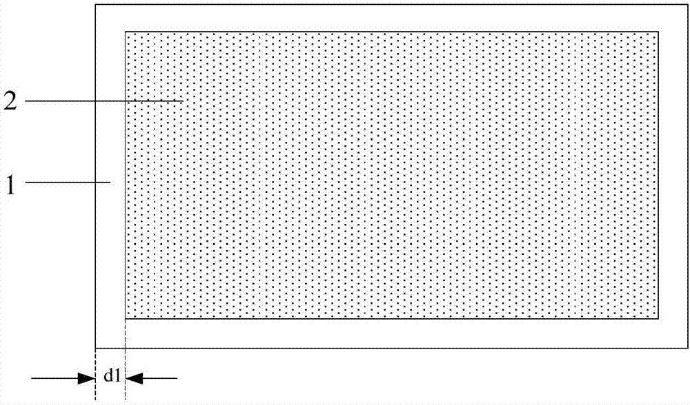
[0045] Step 1, depositing the first thin film 2 on the base substrate 1, there is a first gap d1 between the edge of the first thin film 2 and the edge of the base substrate 1, such as figure 1 shown.
[0046] Specifically, the first thin film 2 is located in the middle of the base substrate 1 . The material of the first thin film 2 can be metal or metal oxide, such as copper, aluminum or indium tin oxide, or single crystal, polycrystal or compound, such as amorphous silicon, silicon nitride or silicon oxide.
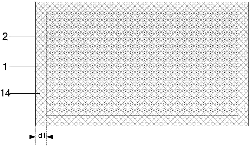
[0047] Step 2, coating photoresist 14 on the first film 2, such as figure 2 shown.
[0048] Specifically, the photoresist 14 is coated on the surface of the base substrate 1 and the first film 2, the photoresist 14 completely c...
Embodiment 2
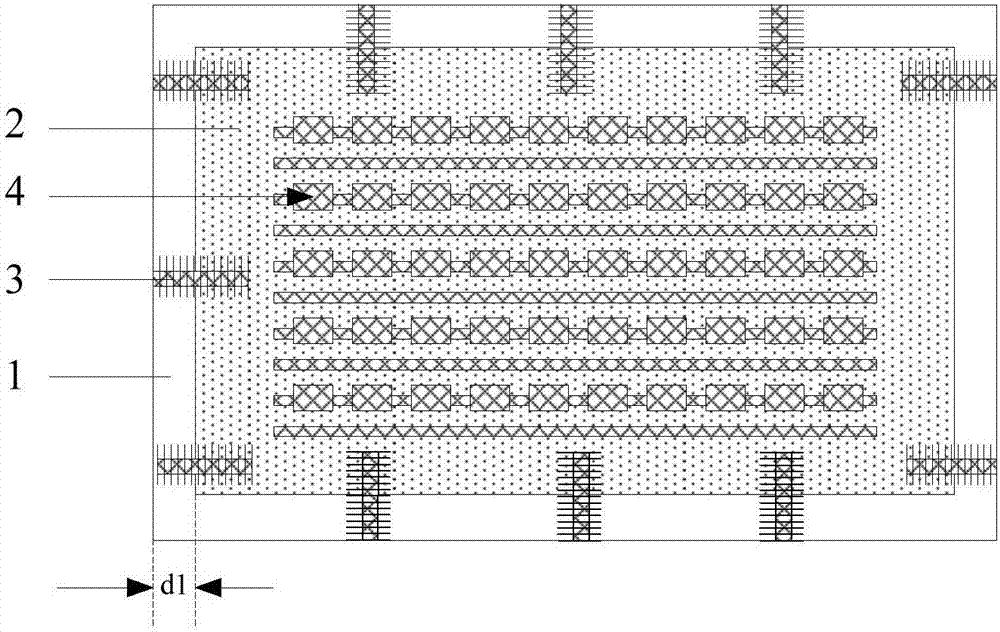
[0064] Embodiment 2 provides an array substrate mother board, combined with Image 6 with Figure 7 As shown, the array substrate motherboard includes a second scale pattern 6 , the second scale pattern 6 is disposed on the base substrate 1 , and there is a gap between the edge of the second scale pattern 6 and the edge of the base substrate 1 .
[0065] Specifically, the second scale pattern 6 includes a plurality of second scale lines 61 and a plurality of second scale values 62, the second scale lines 61 are arranged at equal intervals along the direction perpendicular to the edge of the base substrate 1, and the second scale values 62 and The second scale line 61 corresponds. The distance between adjacent second scale lines 61 is the minimum scale value, preferably, the minimum scale value may be 1-20um.
[0066] In the array substrate motherboard provided by Embodiment 2 of the present invention, after the second film 8 partially covers the second scale pattern 6, a...
Embodiment 3
[0072] Embodiment 3 of the present invention provides a detection method, which is applied to the array substrate motherboard provided in Embodiment 2, such as Figure 8 As shown, the detection method is used to detect the position of the second film 8 formed on the second scale pattern 6 , wherein the second film 8 partially covers the second scale pattern 6 . The method comprises the steps of:
[0073] Step 1, collecting an image of the second scale graphic 6 .
[0074] Specifically, the image of the second scale graphic 6 can be captured by the image acquisition unit 10 , and the image of the second scale graphic 6 can be sent to the image processing unit 11 .
[0075] Preferably, the image acquisition unit 10 includes a transmitting unit and a receiving unit, the transmitting unit is used to transmit an optical signal to the second scale figure 6, and the receiving unit is used to receive the light signal reflected by the second scale figure 6, and the second scale figure...
PUM
 Abstract
Description
Claims
Application Information
 - R&D
- Intellectual Property
- Life Sciences
- Materials
- Tech Scout
- Unparalleled Data Quality
- Higher Quality Content
- 60% Fewer Hallucinations
Browse by: Latest US Patents, China's latest patents, Technical Efficacy Thesaurus, Application Domain, Technology Topic, Popular Technical Reports.
© 2025 PatSnap. All rights reserved.Legal|Privacy policy|Modern Slavery Act Transparency Statement|Sitemap|About US| Contact US: help@patsnap.com