Micro-scale flip LED (Light Emitting Diode) chip and manufacturing method thereof

An LED chip, flip-chip technology, applied in semiconductor/solid-state device manufacturing, electrical components, circuits, etc., can solve problems such as large proportions, and achieve the effects of good current expansion, avoidance of leakage, and high reflectivity

Pending Publication Date: 2017-09-22
SOUTH CHINA UNIV OF TECH
View PDF10 Cites 27 Cited by
  • Summary
  • Abstract
  • Description
  • Claims
  • Application Information

AI Technical Summary

Problems solved by technology

However, for micron-sized LED chips, this protection distance accounts for a large proportion of the chip size, and only about 70% of the light may be reflected from the substrate, while the other 30% of the light is emitted from the p- GaN layer exit

Method used


Image

  • Micro-scale flip LED (Light Emitting Diode) chip and manufacturing method thereof
  • Micro-scale flip LED (Light Emitting Diode) chip and manufacturing method thereof
  • Micro-scale flip LED (Light Emitting Diode) chip and manufacturing method thereof

Examples


Embodiment Construction

[0029] The specific implementation of the present invention will be further described below in conjunction with the accompanying drawings, but the implementation and protection scope of the present invention are not limited thereto.

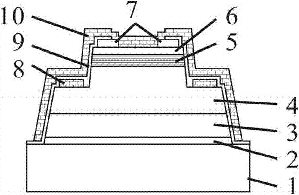
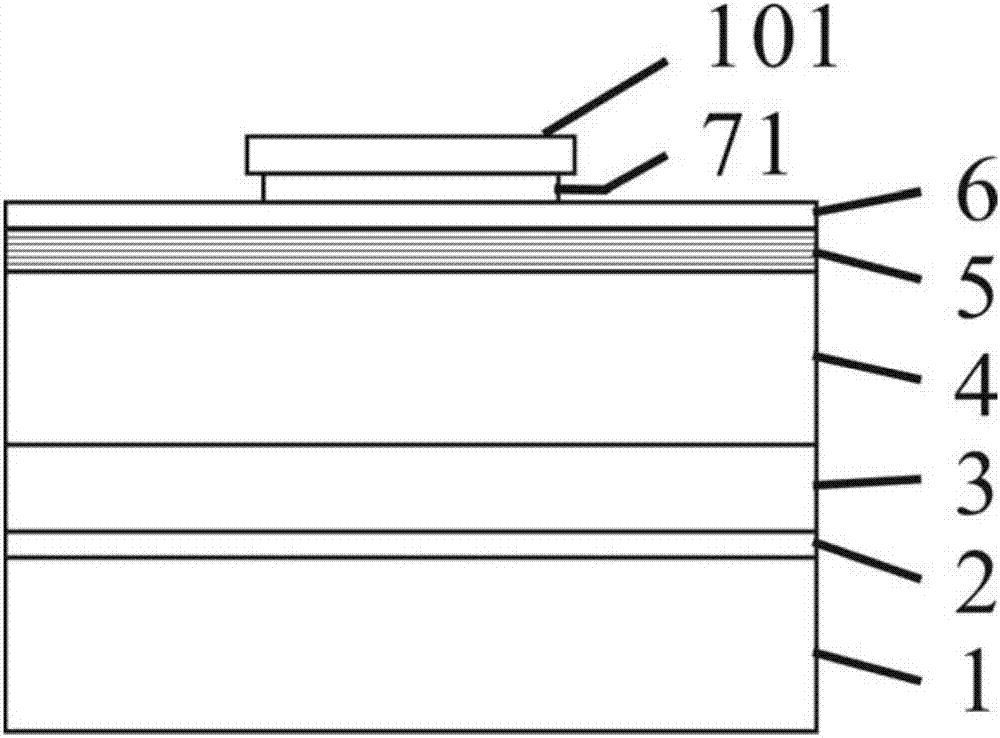
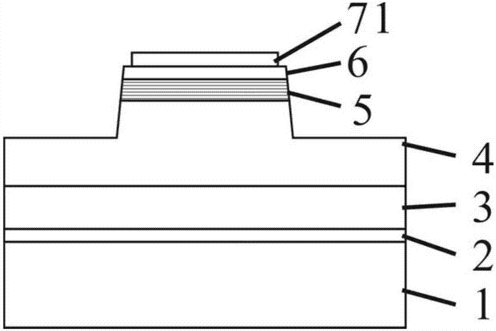
[0030] For a micron-sized flip-chip LED chip structure, such as figure 1 As shown, the substrate 1 is a sapphire material, and the GaN epitaxial layer is composed of a buffer layer 2 , an unintentionally doped GaN layer 3 , an n-GaN layer 4 , a quantum well layer 5 , and a p-GaN layer 6 . The epitaxial layer is a circular truncated structure, an ITO current expansion ring 7 is prepared on the top edge of the mesa, and an n-electrode layer 8 is prepared on the mesa n-GaN layer. A passivation layer 9 is prepared on the side walls of the ITO current expansion ring 7 and the mesa structure, and the passivation layer 9 is SiO 2 insulating layer and SiO 2 / Si 3 N 4 Distributed Bragg reflector composite structure. A p-reflective electrode layer 10 ...


PUM


Abstract

The invention discloses a micro-scale flip LED (Light Emitting Diode) chip and a manufacturing method thereof. A GaN epitaxial layer for manufacturing the LED is of a table structure, both the table base and the table surface of the table structure are in a round table shape, n- electrode rings are distributed on the table base, current spreading rings are distributed at the edge of the top of the table surface, the current spreading material does not diffuse ions at the temperature of 300 DEG C, a passivation layer is arranged on the edge of the top of the current spreading rings and the side wall of the table structure, a dielectric insulating layer and a distributed Bragg reflector layer having the periodic number not smaller than 1 are formed on the passivation layer by adopting chemical vapor deposition, and a p- reflecting electrode layer covers the top of the table surface and the side wall of the passivation layer. The method can improve the reflectivity of a reflector, simultaneously avoids the phenomenon of electric leakage caused by metal diffusion in the reflecting electrode layer, and has relatively large alignment tolerance in the photolithography technique.

Description

technical field [0001] The invention relates to the field of LED chips for visible light communication, in particular to micron-sized flip-chip LED chips and a preparation method thereof. Background technique [0002] In the field of visible light communication, the modulation bandwidth of the LED chip is an important factor affecting the information transmission rate. The modulation bandwidth of the chip is mainly determined by the carrier recombination lifetime and the RC constant, where R and C are the equivalent resistance and equivalent capacitance of the chip, respectively. The use of micron-sized LED chips can reduce the equivalent capacitance and RC constant on the one hand, and on the other hand can increase the current density and reduce the recombination life of minority carriers, thereby improving the modulation bandwidth of the chip. However, compared with ordinary large-sized chips, the ratio of the positive / negative electrode area of ​​the micron-sized chip t...

Claims


Application Information

Patent Timeline
Patent Type & Authority Applications(China)
IPC IPC(8): H01L33/14H01L33/20H01L33/40H01L33/46H01L33/00H01L21/027
CPCH01L33/007H01L33/14H01L33/20H01L33/405H01L33/46H01L21/0274
Inventor 黄华茂王洪杨倬波陈迪涛梁思炜
Owner SOUTH CHINA UNIV OF TECH
Why Eureka
Try Eureka