

Power failure reporting realization method and circuit of power utilization information acquisition equipment
A technology for collecting equipment and power consumption information, applied in the field of electric power, can solve the problems of complex circuit, power consumption, large size, etc., and achieve the effect of simple circuit structure, low cost, and good use effect.
- Summary
- Abstract
- Description
- Claims
- Application Information
AI Technical Summary
Problems solved by technology
Method used
Image

Examples
Embodiment
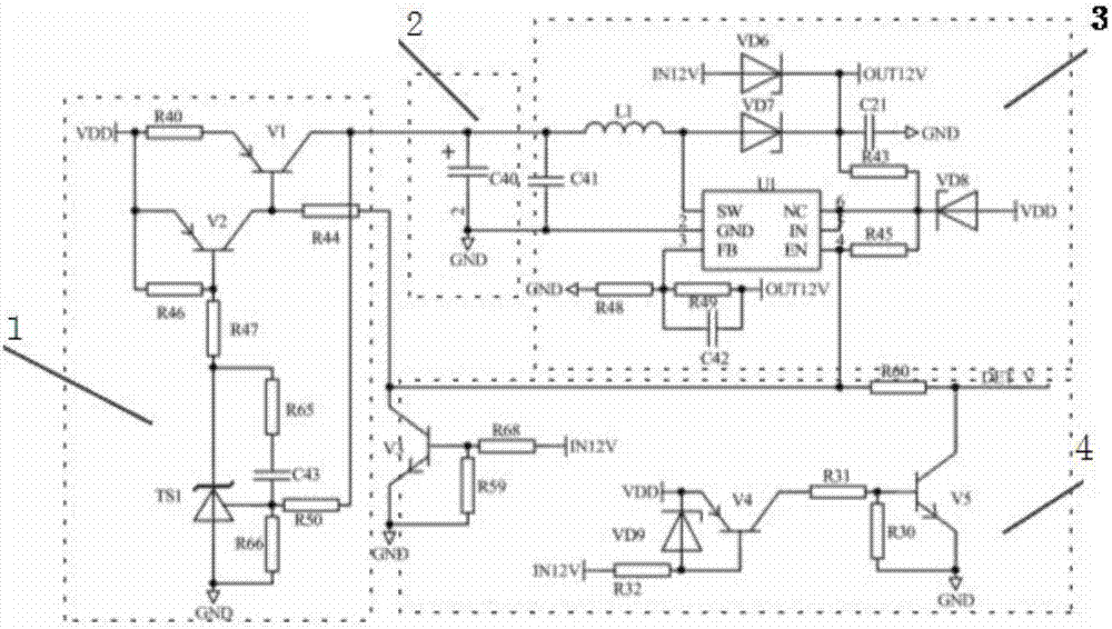
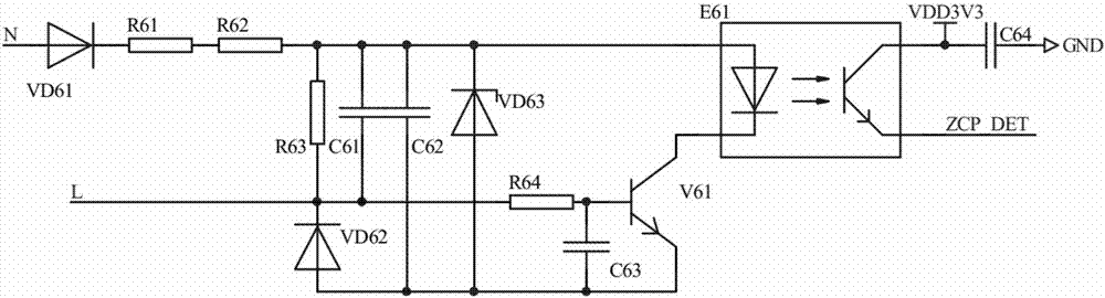
[0023]The implementation method and circuit of the power failure report of the power consumption information collection equipment in this embodiment: In this method, the communication module detects the power supply voltage of the meter and the zero-crossing signal of the power grid to judge the power-off state. When the power-off state is detected, the carrier chip will Detect the zero-crossing signal of the power grid multiple times to judge the power-off state. If there is no zero-crossing signal detected multiple times, it is considered to be in the power-off state, which increases the accuracy of power-off detection; the circuit includes a charging circuit, a farad capacitor, a boost circuit and a power-down Detection and control circuit, the charging circuit is connected to the input voltage VDD; the output of the charging circuit is connected to the farad capacitor; the input of the boost circuit is connected to the farad capacitor; the power-down detection and control ci...
PUM
 Abstract
Description
Claims
Application Information