Short-pulse type D trigger based on FinFET device

A short pulse, trigger technology, applied in pulse generation, pulse technology, electric pulse generation, etc., can solve the problems of high power consumption, complex circuit, short signal width, etc.

Active Publication Date: 2017-09-29
NINGBO UNIV
View PDF6 Cites 7 Cited by
  • Summary
  • Abstract
  • Description
  • Claims
  • Application Information

AI Technical Summary

Problems solved by technology

The circuit diagram of a traditional pulse-type D flip-flop is as follows figure 1 As shown, the pulse-type D flip-flop adopts CMOS design, the circuit is complicated, the number of FinFET tubes required is large, the power consumption is large, and a feedback path is required, so that an additional clock-controlled clock transmission tube is required to avoid short-circuit power consumption, which is not conducive to Low Power Design
At the same time, since the output pulse signal is obtained through the delay of the two-stage inverter, the signal width is very short

Method used


Image

  • Short-pulse type D trigger based on FinFET device
  • Short-pulse type D trigger based on FinFET device
  • Short-pulse type D trigger based on FinFET device

Examples


Embodiment 1

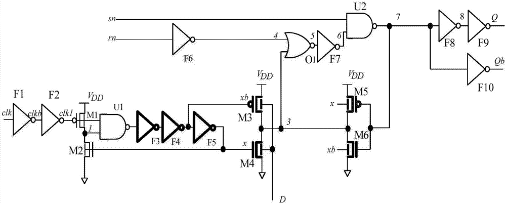
[0030] Embodiment one: if figure 2 As shown, a short-pulse D flip-flop based on FinFET devices includes a first FinFET tube M1, a second FinFET tube M2, a third FinFET tube M3, a fourth FinFET tube M4, a fifth FinFET tube M5, and a sixth FinFET tube Tube M6, first inverter F1, second inverter F2, third inverter F3, fourth inverter F4, fifth inverter F5, sixth inverter F6, seventh inverter F7, the eighth inverter F8, the ninth inverter F9, the tenth inverter F10, the first two-input NOR gate O1, the first two-input NAND gate U1 and the second two-input NAND gate U2; The first two-input NOR gate O1, the first two-input NOR gate O1 and the second two-input NAND gate U2 respectively have a first input terminal, a second input terminal and an output terminal; the first FinFET tube M1, the third FinFET The tube M3 and the fifth FinFET tube M5 are all P-type FinFET tubes, the second FinFET tube M2, the fourth FinFET tube M4 and the sixth FinFET tube M6 are all N-type FinFET tubes, ...

Embodiment 2

[0031] Embodiment two: if figure 2As shown, a short-pulse D flip-flop based on FinFET devices includes a first FinFET tube M1, a second FinFET tube M2, a third FinFET tube M3, a fourth FinFET tube M4, a fifth FinFET tube M5, and a sixth FinFET tube Tube M6, first inverter F1, second inverter F2, third inverter F3, fourth inverter F4, fifth inverter F5, sixth inverter F6, seventh inverter F7, the eighth inverter F8, the ninth inverter F9, the tenth inverter F10, the first two-input NOR gate O1, the first two-input NAND gate U1 and the second two-input NAND gate U2; The first two-input NOR gate O1, the first two-input NOR gate O1 and the second two-input NAND gate U2 respectively have a first input terminal, a second input terminal and an output terminal; the first FinFET tube M1, the third FinFET The tube M3 and the fifth FinFET tube M5 are all P-type FinFET tubes, the second FinFET tube M2, the fourth FinFET tube M4 and the sixth FinFET tube M6 are all N-type FinFET tubes, t...


PUM


Abstract

The invention discloses a short-pulse type D trigger based on FinFET device. The short-pulse type D trigger comprises a first FinFET tube, a second FinFET tube, a third FinFET tube, a fourth FinFET tube, a fifth FinFET tube, a sixth FinFET tube, a first phase inverter, a second phase inverter, a third phase inverter, a fourth phase inverter, a fifth phase inverter, a sixth phase inverter, a seventh phase inverter, a seventh phase inverter, an eighth phase inverter, a ninth phase inverter, a tenth phase inverter, a first two-input NOR gate, a first two-input XOR gate and a second two-input XOR gate, wherein each of the first two-input NOR gate, the first two-input XOR gate and the second two-input XOR gate is provided with a first input, a second input and an output end; the short-pulse type D trigger has the advantages that the number of the FinFET tube is reduced, the circuit delay and the circuit area are further optimized since the series connection of the transistor is reduced; therefore, the circuit area, the time delay, the power consumption and the power delay product are small under the condition of not influencing the circuit performance.

Description

technical field [0001] The invention relates to a short-pulse D flip-flop, in particular to a short-pulse D flip-flop based on a FinFET device. Background technique [0002] As the size of transistors continues to shrink, limited by the short-channel effect and the current manufacturing process, the space for reducing the size of ordinary CMOS transistors is extremely narrowed. When the size of an ordinary CMOS transistor is reduced to below 20nm, the leakage current of the device will increase sharply, resulting in a large leakage power consumption of the circuit. Moreover, the short-channel effect of the circuit becomes more obvious, and the device becomes quite unstable, which greatly limits the improvement of the circuit performance. [0003] In VLSI, the power consumption of the clock system accounts for almost one-third of the total power consumption of the circuit. In the clock system, the power consumption generated by the flip-flop and the buffer directly driving ...

Claims


Application Information

Patent Timeline
Patent Type & Authority Applications(China)
IPC IPC(8): H03K3/3562
CPCH03K3/3562
Inventor 胡建平朱昊天杨廷锋
Owner NINGBO UNIV
Why Eureka
Try Eureka