A CSP chip with no step electrode structure and its manufacturing method
A step electrode and chip technology, applied in circuits, electrical components, semiconductor devices, etc., can solve problems such as poor sticking effect, increased complexity, leakage, etc., to avoid the aging and cracking of glue and silver glue, and save costs. And the process flow, the effect of simple production process
- Summary
- Abstract
- Description
- Claims
- Application Information
AI Technical Summary
Problems solved by technology
Method used
Image
Examples
Embodiment Construction
[0027] One, the manufacturing steps of the present invention are as follows:
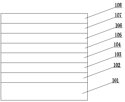
[0028] 1. If figure 1 As shown, the transition layer 102, the GaN current spreading layer 103, the N-GaN confinement layer 104, the MQW multi-quantum well active layer 105, the Al-GaN confinement layer 106, and the P-GaN A current spreading layer 107 and an In-GaN ohmic contact layer 108 .
[0029] Wherein the GaN current spreading layer 103 preferably has a thickness of 60nm, the doped impurity element is Si, and the doping concentration is 8×10 18 cm -3 above to ensure a good electrical contact on the N side.
[0030] In-GaN ohmic contact layer 108 preferably has a thickness of 3000nm, the doped impurity element is Mg, and the doping concentration is 7×10 18 cm -3 above to ensure a good electrical contact on the P side.
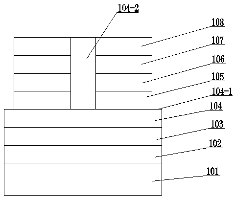
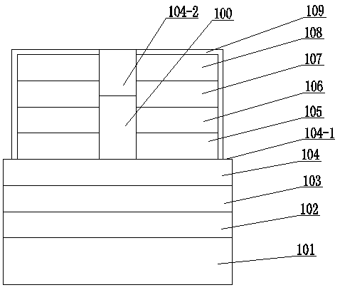
[0031] 2. Use 511 cleaning solution to clean the In-GaN ohmic contact layer 108, spin-coat positive photoresist, make a mask pattern through exposure and development, and t...
PUM
 Abstract
Description
Claims
Application Information


