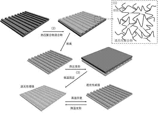
Preparation method of shape memory polymer film for automatically adjusting transparency according to indoor temperature
A memory polymer, indoor temperature technology, applied in the direction of flat products, other household appliances, household appliances, etc., can solve the problem of high cost, achieve the effect of improving the living environment and good application prospects
- Summary
- Abstract
- Description
- Claims
- Application Information
AI Technical Summary
Problems solved by technology
Method used
Image
Examples
preparation example Construction
[0043] In the step 1), the preparation method of the reversible shape memory polymer comprises the following steps:
[0044] 1.1) Dissolve the semi-crystalline polymer and plasticizer in dichloromethane at a mass ratio of 4-7:1;
[0045] 1.2) Then the dissolved solution is concentrated by rotary evaporation;
[0046] 1.3) Precipitation with anhydrous ether and vacuum drying to obtain a homogeneous mixture of poly(1,4-butene adipate) and benzyl cinnamic acid;
[0047] 1.4) The mixture was vacuum-dried again to constant weight.
[0048] In the step 2), the micropattern on the surface of the silicon wafer template is prepared by photolithography, soft etching or thermal embossing process.
[0049] In the step 2), the micropattern on the surface of the silicon wafer template is a composite pattern formed by a lattice.
[0050] The lattice unit is straight arc, circular or polygonal grooves or protrusions in micron or nanometer scale.
[0051] In the step 2), the pouring method...
Embodiment 1
[0061] The preparation of a light-transmitting polymer film that can be freely adjusted according to the indoor temperature of the present invention is divided into the following steps:
[0062] Dissolve 10g of poly(1,4-butene adipate) and 2g of benzyl cinnamic acid in 30mL of dichloromethane in a certain proportion, concentrate by rotary evaporation, precipitate with anhydrous ether and dry in vacuo to obtain A homogeneous mixture of white powder poly(1,4-butene adipate) and benzyl cinnamic acid, vacuum-dried to constant weight; using photolithography technology, a silicon wafer template with a diameter of 50 μm was prepared on the surface ; Then place the micropattern on the bottom, cover the resulting mixture on the silicon wafer, and place the whole in a hot press mold. The temperature of the hot press is increased to 60 ° C, the pressure is increased to 4 MPa, and kept for 20 minutes to make the polymer The material penetrates into the silicon wafer template; after the te...
Embodiment 2
[0066] This example is basically the same as Example 1, except that the pattern on the surface of the silicon wafer template by photolithography technology is a groove structure with a diameter and a height of 30 μm.
PUM
| Property | Measurement | Unit |
|---|---|---|
| diameter | aaaaa | aaaaa |
| height | aaaaa | aaaaa |
Abstract
Description
Claims
Application Information
