Check patentability & draft patents in minutes with Patsnap Eureka AI!

Bi-directional bootstrapped dynamic switching circuit with high-voltage device working under low voltage

A technology of dynamic switches and high-voltage devices, which is applied in the direction of electronic switches, circuits, semiconductor devices, etc., can solve the problems of transmission gate speed influence, high cost, and decreased precision, and achieve the effects of reducing parasitic effects, reducing costs, and increasing speed

Pending Publication Date: 2017-10-17
SHENZHEN BETTERLIFE ELECTRONICS SCI & TECH
View PDF0 Cites 2 Cited by
  • Summary
  • Abstract
  • Description
  • Claims
  • Application Information

AI Technical Summary

Problems solved by technology

[0010] Since the fingerprint identification chip is designed as a 5V medium-voltage device, the minimum operating voltage is only about 2.4V, and the V of the 5V device TH It is close to 1.0V, so if a conventional transmission gate is used, the size of the NMOS tube and the PMOS tube will be very large, which will bring the following disadvantages: first, the size and area of ​​the NMOS tube and the PMOS tube of the transmission gate are large; , due to the large area of ​​the transmission gate circuit, the corresponding parasitic capacitance and other parameters are also large, which affects the speed of the transmission gate; at the same time, the large size also brings high cost problems. In addition, due to the large size of the transmission gate, the closing When turned on, it will cause a large clock feedthrough, which will increase the error and reduce the accuracy

Method used


Image

  • Bi-directional bootstrapped dynamic switching circuit with high-voltage device working under low voltage
  • Bi-directional bootstrapped dynamic switching circuit with high-voltage device working under low voltage
  • Bi-directional bootstrapped dynamic switching circuit with high-voltage device working under low voltage

Examples


Embodiment Construction

[0021] The present invention will be described in more detail below in conjunction with the accompanying drawings and embodiments.

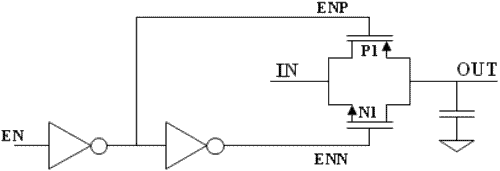
[0022] The invention discloses a bidirectional bootstrap dynamic switch circuit in which a high-voltage device works at a low voltage, such as figure 2 As shown, it includes a first NOT gate U1, a second NOT gate U2, a first capacitor C1, a second capacitor C2, a first PMOS transistor P1, a second PMOS transistor P2, a third PMOS transistor P3, and a fourth PMOS transistor P4, the first NMOS transistor N1, the second NMOS transistor N2, the third NMOS transistor N3, the fourth NMOS transistor N4, and the bootstrap capacitor CH, the first invertor U1 and the second invertor U2 are connected in series in sequence, and the first invertor U1 and the second invertor U2 are serially connected The input terminal of a NOT gate U1 is used to access the clock pulse signal, wherein:

[0023] The output end of the second NOT gate U2 is connected to the fro...


PUM


Abstract

The invention discloses a bi-directional bootstrapped dynamic switching circuit with a high-voltage device working under low voltage, wherein the output end of a second NOT gate is connected with the front end of a first capacitor, the rear end of the first capacitor and the drain of a second PMOS transistor are connected with the source of a third PMOS transistor, both the grid of the third PMOS transistor and the grid of a second NMOS transistor are connected with the output end of the first NOT gate, the grid of the second PMOS transistor, the drain of the third PMOS transistor and the drain of the second NMOS transistor are connected with the grid of a first NMOS transistor; the output end of the first NOT gate is connected with the front end of a second capacitor, the rear end of the second capacitor and the source of the third NMOS transistor are connected with the drain of a fourth NMOS transistor, the grid of a fourth PMOS transistor, the grid of the third NMOS transistor and the grid of the fourth NMOS transistor are connected with the output end of the first NOT gate, and the drain of the fourth PMOS transistor and the drain of the third NMOS transistor are connected with the grid of the first PMOS transistor. According to the circuit provided by the invention, the size of a transmission gate can be effectively reduced, the speed of the transmission gate can be effectively improved, clock feedthrough can be effectively reduced, error can be effectively reduced and accuracy can be effectively improved.

Description

technical field [0001] The invention relates to a circuit structure for realizing high-speed switching in a low-voltage environment, in particular to a bidirectional bootstrap dynamic switching circuit in which a high-voltage device operates at a low voltage. Background technique [0002] In the prior art, the common CMOS switch transmission gate circuit is composed of a PMOS transistor and an NMOS transistor, please refer to figure 1 , by adding ENN (VDDA) to the Gate pole of the NMOS transistor and ENP (VSSA) to the Gate pole of the PMOS transistor to realize low-impedance conduction input and output, when the input and output voltages are constant, the higher the power supply voltage of the circuit, the higher the transmission The smaller the on-resistance of the gate, the faster the transmission speed. When designing a high-speed switched-capacitor circuit, the on-resistance of the transmission gate circuit must be low enough if the signal needs to be transmitted quickl...

Claims


Application Information

Patent Timeline
IPC IPC(8): H03K17/042H03K17/687
CPCH03K17/04206H03K17/687
Inventor 陈思伟余佳
Owner SHENZHEN BETTERLIFE ELECTRONICS SCI & TECH
Features
  • R&D
  • Intellectual Property
  • Life Sciences
  • Materials
  • Tech Scout
  • Unparalleled Data Quality
  • Higher Quality Content
  • 60% Fewer Hallucinations
Learn More