Wave soldering clamp and method for optical device

A technology of wave soldering and optical devices, applied in welding equipment, auxiliary welding equipment, welding/cutting auxiliary equipment, etc., can solve problems such as low production efficiency, damage to optical devices, hidden quality problems, etc., to improve production efficiency and welding efficiency , Guarantee the effect of welding quality

Active Publication Date: 2017-10-20
湖北兆元科技有限公司
View PDF6 Cites 8 Cited by
  • Summary
  • Abstract
  • Description
  • Claims
  • Application Information

AI Technical Summary

Problems solved by technology

Optical device welding generally adopts a streamlined production method, but at present, optical device welding is prone to poor welding, and the temperature is high during welding, which is likely to cause damage to optical devices, resulting in hidden quality problems and low production efficiency

Method used


Image

  • Wave soldering clamp and method for optical device
  • Wave soldering clamp and method for optical device
  • Wave soldering clamp and method for optical device

Examples


Embodiment Construction

[0025] The present invention will be further described in detail below in conjunction with the accompanying drawings and specific embodiments.

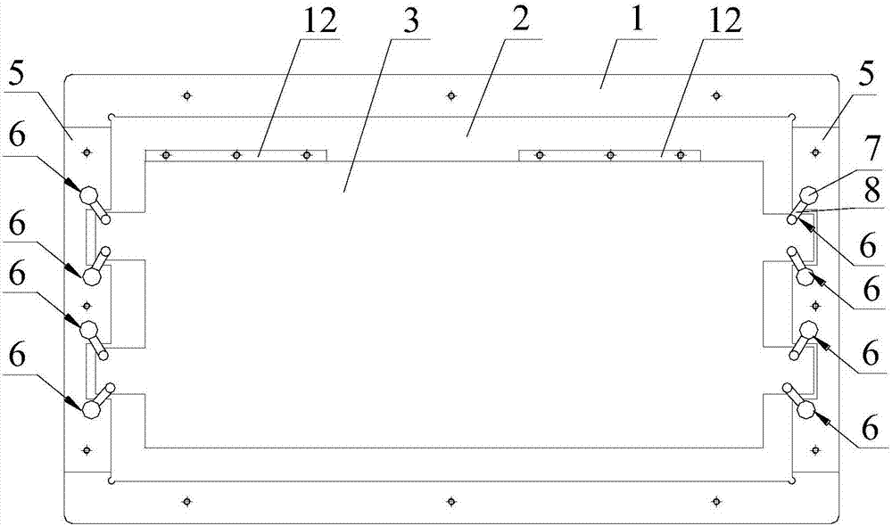
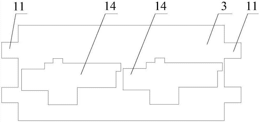
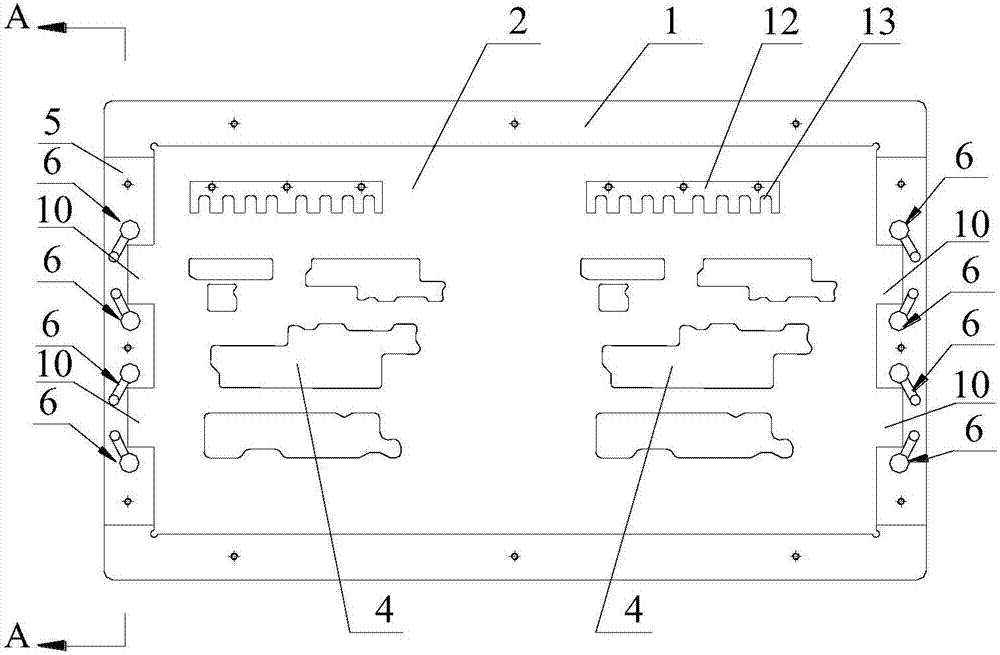
[0026] see figure 1 As shown, the embodiment of the present invention provides a wave soldering fixture for optical devices, which is used for soldering optical devices to a PCB board. The fixture includes a frame 1, a bottom plate 2 and a cover plate 3. Welding holes 4 for device welding, at least one clamping assembly 6 is provided on both sides of the frame 1, the cover plate 3 is covered on the bottom plate 2 through the clamping assembly 6, and at least one PCB board can be placed between the bottom plate 2 and the cover plate 3 The side of the cover plate 3 close to the PCB board is provided with at least one relief groove 14, and the shape of the relief groove 14 matches the optical device on the PCB board. At least one LED lamp positioning plate 12 is provided on the bottom plate 2 , and several LED lamp positioning grooves 1...


PUM


Abstract

The invention discloses a wave soldering clamp and method for an optical device and relates to the field of wave soldering clamps. The clamp is used for soldering the optical device on a PCB (Printed Circuit Board); the clamp comprises an edge frame, a bottom plate and a cover plate, wherein the edge frame is fixedly connected with the bottom plate; the bottom plate is provided with at least one soldering hole for soldering the optical device; at least one clamping assembly is arranged at each of two sides of the edge frame; the cover plate covers the bottom plate through the clamping assemblies; at least one PCB can be arranged between the bottom plate and the cover plate; at least one yielding groove is formed in one side, close to the PCB, of the cover plate; the shape of the yielding groove is matched with the shape of the optical device on the PCB; the bottom plate is provided with at least one LED (Light Emitting Diode) lamp positioning plate; and a plurality of LED lamp positioning grooves are formed in the LED lamp positioning plate. The method comprises steps of putting the PCB in the clamp and then carrying out automatic wave soldering. By adopting the wave soldering clamp and method for the optical device, disclosed by the invention, the soldering quality of the optical device can be ensured and the soldering efficiency of the optical device is improved.

Description

technical field [0001] The invention relates to the field of wave soldering fixtures, in particular to a wave soldering fixture for optical devices and a welding method thereof. Background technique [0002] Wave soldering technology has been widely used in batch soldering of optical devices. The soldering surface of the plug-in board is directly in contact with the high-temperature liquid tin to achieve the purpose of soldering. The high-temperature liquid tin maintains an inclined plane, and the liquid tin is formed into waves by special devices. Phenomenon, so it is called "wave soldering", and its main material is solder bar. [0003] Optical devices are divided into active devices and passive devices. Optical active devices are optoelectronic devices that require external energy to work in optical communication systems and can convert electrical signals into optical signals or convert optical signals into electrical signals. , is the heart of the optical transmission s...

Claims


Application Information

Patent Timeline
Patent Type & Authority Applications(China)
IPC IPC(8): B23K3/08B23K37/04B23K1/08
CPCB23K1/085B23K3/087
Inventor 王标
Owner 湖北兆元科技有限公司
Why Eureka
Try Eureka