
Power semiconductor chip and photomask and exposure method of chip

A power semiconductor and lithography technology, applied in the field of power electronics, can solve the problems of inability to apply complex structure chips, increasing the number of lithography plates, and not considering key dimensions, etc., to achieve the effect of simple graphics, reducing the number of use, and improving errors

Active Publication Date: 2017-11-03
ZHUZHOU CRRC TIMES SEMICON CO LTD
View PDF7 Cites 3 Cited by
  • Summary
  • Abstract
  • Description
  • Claims
  • Application Information

AI Technical Summary

Problems solved by technology

[0010] In view of this, the purpose of the present invention is to provide a power semiconductor chip, the photolithographic plate of the chip and its exposure method, to solve the problem that the existing chip is made by directly splicing multiple plates, resulting in an increase in the number of photolithographic plates and a high cost. increase, and the key size of the graphics at the splicing point is not considered when splicing directly, which is likely to cause splicing errors and cannot be applied to the technical problems of chip preparation with complex structures

Method used


Image

  • Power semiconductor chip and photomask and exposure method of chip
  • Power semiconductor chip and photomask and exposure method of chip
  • Power semiconductor chip and photomask and exposure method of chip

Examples


Embodiment 1

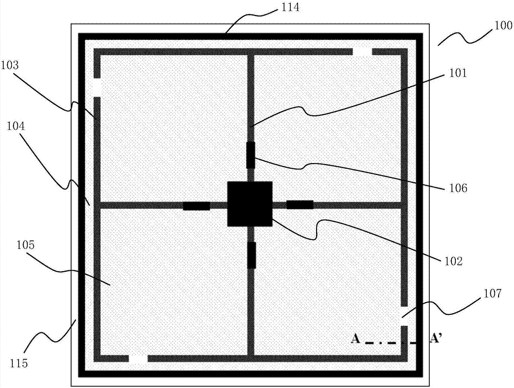
[0062] as attached figure 1 As shown, a specific embodiment of a power semiconductor chip includes: a termination region 114 , and an emitter region and a gate region located in the termination region 114 . The emitter region includes a peripheral emitter region 104 and a plurality of main emitter regions 105 , and the gate region includes a gate bar 101 , a main gate region 102 , a peripheral gate 103 and a gate resistor 106 . The peripheral gate 103 is located on the periphery of the main gate region 102 , and the peripheral gate 103 is discontinuous. The main gate region 102 is located in the center of the area surrounded by the peripheral gate 103 , and the peripheral gate 103 is connected to the main gate region 102 through a gate bar 101 , and a gate resistor 106 is arranged on the gate bar 101 . The shape of the main gate region 102 may be a centrosymmetric figure such as a circle, a square, or a regular polygon. The peripheral grid 103 includes disconnection points 1...

Embodiment 2

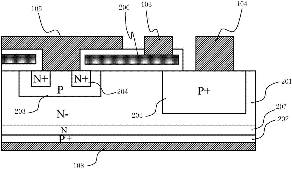
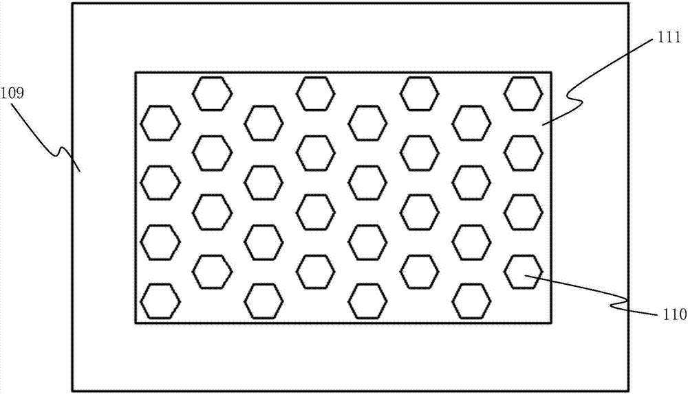
[0066] as attached Figure 4 As shown, on the basis of Embodiment 1, the emitter region and the gate region on the front of the chip 100 are further formed with a first metallization layer 109 through a metallization process, and a dielectric layer 112 is provided on the first metallization layer 109, The dielectric layer 112 does not extend beyond the first metallization layer 109 . Setting the dielectric layer 112 can raise the step of the channel region of the cell 200 , and can reduce the pressure on the channel region during chip bonding, so that the gate oxide layer 208 of the channel is not easily damaged. Dielectric layer through holes 110 are provided in the dielectric layer 112 located in the main emitter region 105 and the main gate region 102 . A second metallization layer 111 is disposed on the dielectric layer 112 , and the second metallization layer 111 is connected to the first metallization layer 109 through the dielectric layer via hole 110 . The range of t...

Embodiment 3

[0070] A specific embodiment of a photolithography plate of a power semiconductor chip. The pattern of the chip 100 described in the above embodiment 1 and embodiment 2 is divided into four equal parts with the gate bar 101 as the axis of symmetry, which are respectively the first area A0, The second area A1, the third area A2 and the fourth area A3. The patterns of the gate strip 101 and the main gate region 102 are located at the pattern splicing position, and the pattern of the photolithography plate 300 is the same as any of the equally divided patterns, as shown in the attached Figure 5 shown. The cell area does not participate in the splicing of graphics due to its small line width and complex graphics. To ensure the integrity of the pattern splicing, the edge of the photoresist plate 300 located at the adjacent pattern splicing position is also provided with an overlapping area 113 extending toward the splicing direction, as shown in the attached Figure 7 shown. as...


PUM

PropertyMeasurementUnit
thicknessaaaaaaaaaa
thicknessaaaaaaaaaa
thicknessaaaaaaaaaa

Abstract

The invention discloses a power semiconductor chip and a photomask and exposure method of the chip. The chip comprises a terminal region, an emitter region and a grid region, wherein the emitter region and the grid region are arranged in the terminal region, the emitter region comprises a periphery and main emitter regions, the grid region comprises grid strips, a main grid region, a peripheral grid and grid resistors, the peripheral grid is arranged at the periphery of the main grid region, the main grid region is arranged in the center of a region encircled by the peripheral grid, the peripheral grid is connected with the main grid region through the grid strips and the grid resistors and comprises breaking points, the breaking points are arranged in a central symmetric and / or axial symmetric structure, the region encircled by the peripheral grid is partitioned into a plurality of main emitter regions with same size by the grid strips, and each main emitter region communicates with the peripheral emitter region arranged at the periphery of the peripheral grid through the breaking points. By the chip, the technical problems that many photomasks are used, the cost is high, a splicing error is easy to generate and the chip cannot be used for fabricating a complicated-structure chip during fabrication of a large-size chip by employing a plurality of plates to splice can be solved.

Description

technical field [0001] The invention relates to the technical field of power electronics, in particular to a power semiconductor chip, a photolithography plate of the chip and an exposure method thereof. Background technique [0002] With the development of technology and the continuous expansion of application fields, power semiconductor devices occupy an increasingly important position in modern power electronics technology. At present, power semiconductor devices are developing in the direction of high frequency, high power, intelligence and modularization. Among them, as a key technology for the application of power semiconductor devices, how to realize the high power capacity of power semiconductor modules has become the key direction of research and development in this technical field. [0003] In order to realize the high power capacity of the power semiconductor module, in the prior art, several or even a dozen small chips are usually packaged in parallel to form a ...

Claims


Application Information

Patent Timeline
Patent Type & Authority Applications(China)
IPC IPC(8): G03F7/20G03F1/42H01L29/739H01L29/08H01L29/10H01L21/331
CPCG03F1/42G03F7/70475G03F9/7073H01L29/0804H01L29/10H01L29/66325H01L29/7393
Inventor 王梦洁刘国友程银华喻乐贤陈辉谭灿健肖强罗海辉黄建伟覃荣震
Owner ZHUZHOU CRRC TIMES SEMICON CO LTD
Learn More