A method for detecting registration deviation of ion-implanted layer patterns

A technology of ion implantation and registration deviation, which is applied in semiconductor/solid-state device testing/measurement, electrical components, circuits, etc., and can solve problems such as registration deviation cannot be confirmed

Inactive Publication Date: 2020-08-28
NANJING LISHUI HIGH-TECH VENTURE CAPITAL MANAGEMENT CO LTD
View PDF3 Cites 0 Cited by
  • Summary
  • Abstract
  • Description
  • Claims
  • Application Information

AI Technical Summary

Problems solved by technology

[0003] In the semiconductor chip manufacturing process, for the graphic layer that needs to be ion-implanted, because the photoresist layer used as the shielding layer will be removed after ion implantation, so when the electrical parameters of the product are finally tested, if there is an abnormality, the ion Injected misregistration issues cannot be confirmed at this time
Although the pattern registration deviation measurement is generally performed during the photolithography process of the ion implantation layer, the above pattern registration deviation measurement is a sampling test, which does not mean that the pattern registration of all areas on the wafer is normal

Method used


Image

  • A method for detecting registration deviation of ion-implanted layer patterns
  • A method for detecting registration deviation of ion-implanted layer patterns
  • A method for detecting registration deviation of ion-implanted layer patterns

Examples


Embodiment Construction

[0026] The following will clearly and completely describe the technical solutions in the embodiments of the present invention. Obviously, the described embodiments are only some of the embodiments of the present invention, rather than all the embodiments. Based on the embodiments of the present invention, all other embodiments obtained by persons of ordinary skill in the art without making creative efforts belong to the protection scope of the present invention.

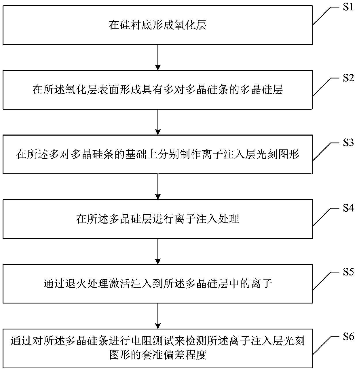
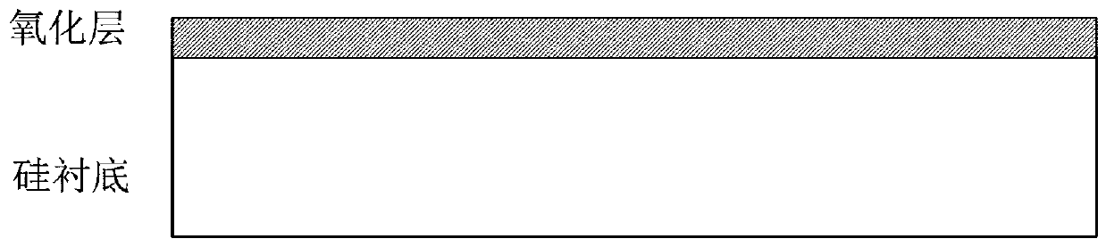
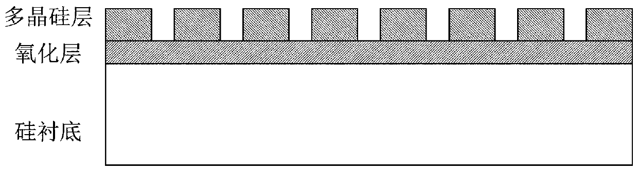
[0027] In order to solve the problem in the prior art that the registration deviation of the photolithography pattern of the ion implantation layer cannot be determined during the manufacturing process of the semiconductor chip, the present invention provides a detection method for the registration deviation of the ion implantation layer pattern, which can provide the ion implantation layer electric current The electrical test structure ensures that the registration of the photolithography pattern of the ion implantat...


PUM

PropertyMeasurementUnit
thicknessaaaaaaaaaa
thicknessaaaaaaaaaa

Abstract

The invention provides a method for detecting a pattern registration deviation of an ion implanted layer. The method for detecting the pattern registration deviation of the ion implanted layer comprises the steps of: forming a polycrystalline silicon layer with a plurality of pairs of polycrystalline silicon strips on the surface of an oxide layer; respectively fabricating ion implanted layer etched patterns on the basis of the plurality of pairs of polycrystalline silicon strips; carrying out ion implantation processing on the polycrystalline silicon layer; and by carrying out resistance testing on the plurality of pairs of polycrystalline silicon strips, detecting a registration deviation condition of the ion implanted layer etched patterns. By providing an ion implanted layer electrical testing structure, the method provided by the invention can ensure that in an electrical testing measurement stage of a product, the registration deviation degree of the ion implanted layer etched patterns can be reflected by measuring electrical parameters of the ion implanted layer.

Description

【Technical field】 [0001] The invention relates to the technical field of semiconductor chip manufacturing, in particular to a detection method for pattern registration deviation of an ion implantation layer. 【Background technique】 [0002] In the electronics industry, ion implantation is a very important doping technology in the semiconductor manufacturing process, and it is also an important means to control the threshold voltage of transistors. In the manufacturing process of contemporary semiconductor chips, especially large-scale integrated circuit chips, ion implantation technology can be said to be an indispensable means. [0003] In the semiconductor chip manufacturing process, for the graphic layer that needs to be ion-implanted, because the photoresist layer used as the shielding layer will be removed after ion implantation, so when the electrical parameters of the product are finally tested, if there is an abnormality, the ion Injected misregistration issues canno...

Claims


Application Information

Patent Timeline
Patent Type & Authority Patents(China)
IPC IPC(8): H01L21/66
CPCH01L22/12H01L22/14
Inventor 张婉婷
Owner NANJING LISHUI HIGH-TECH VENTURE CAPITAL MANAGEMENT CO LTD
Why Eureka
Try Eureka