Method for detecting dislocation density of semiconductor chip

A detection method and semiconductor technology, applied in measurement devices, optical testing of flaws/defects, material analysis by optical means, etc. The effect of high measurement speed, high analysis speed and high scanning accuracy

Inactive Publication Date: 2017-11-17
THE 13TH RES INST OF CHINA ELECTRONICS TECH GRP CORP
View PDF4 Cites 2 Cited by
  • Summary
  • Abstract
  • Description
  • Claims
  • Application Information

AI Technical Summary

Problems solved by technology

Since the metallographic microscope cannot distinguish the vertical depth of the corrosion pit, it can only be manually judged by the two-dimensional surface pattern of the S pit and the D pit. Usually, it is necessary to manually distinguish the image point by point, which is time-consuming, laborious, and inconvenient. Pit and S pits are also more difficult, so there are large errors in statistics
For wafers with low dislocation density, it is easy to cause missing numbers with traditional metallographic microscopes, and the measured value deviates greatly from the actual value.

Method used


Image

  • Method for detecting dislocation density of semiconductor chip
  • Method for detecting dislocation density of semiconductor chip
  • Method for detecting dislocation density of semiconductor chip

Examples


Embodiment Construction

[0022] The present invention will be further described in detail below in conjunction with the accompanying drawings and specific embodiments.

[0023] The detection method of semiconductor wafer dislocation density provided by the invention comprises the following steps:

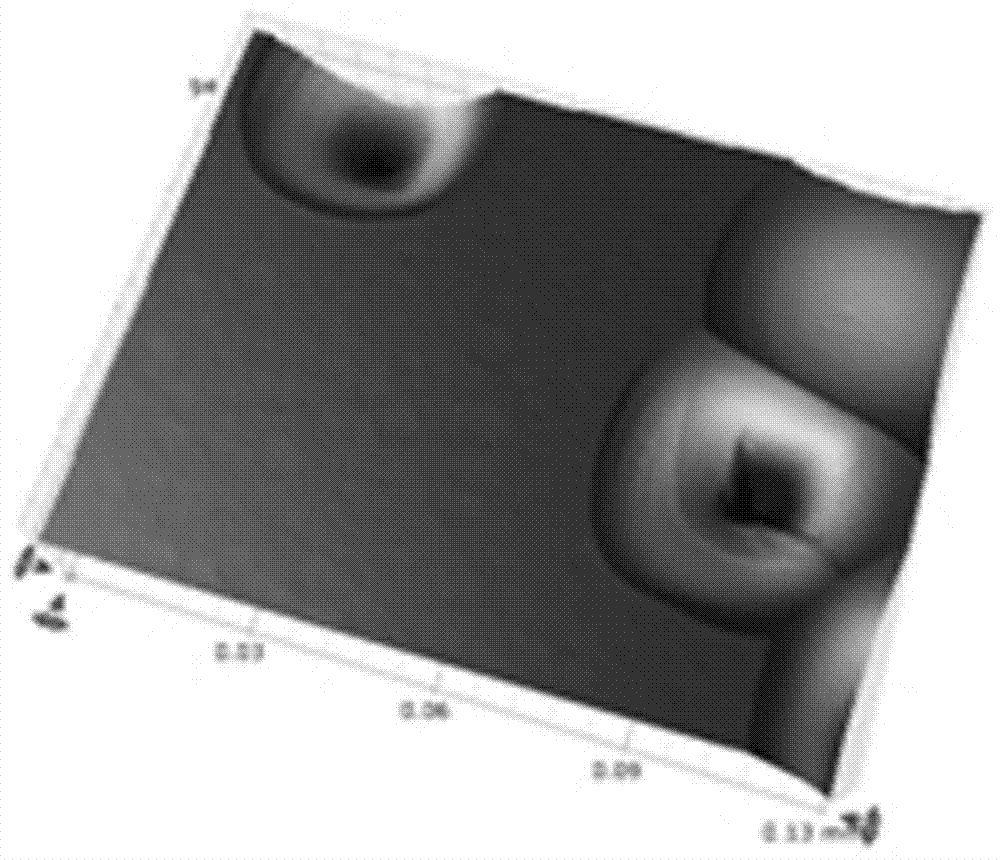
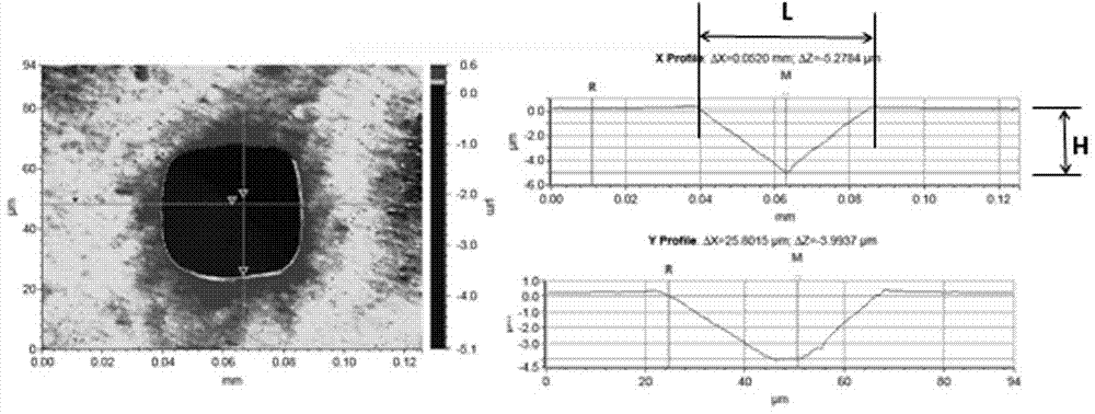
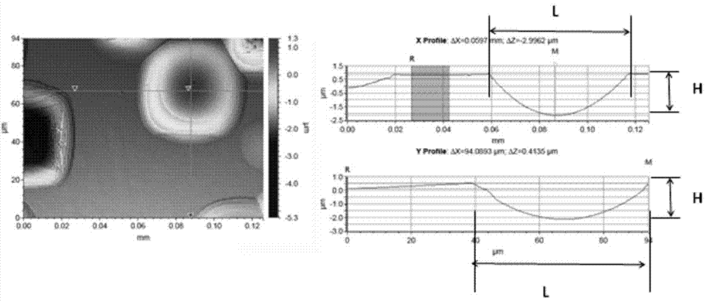
[0024] 1) Put the corroded sample on the white light interferometer for scanning, set the upper and lower margins of the scan and the number of scanning points, the principle of the white light interferometer is as follows Figure 5 shown;

[0025] 2) Scan image by image: fine-tune each image to make the interference fringe clearer;

[0026] 3) Automatic data statistics: automatically identify dislocation corrosion pits, and automatically count the number of dislocation corrosion pits in each image, and calculate the dislocation density;

[0027] 4) Generate a test report: The dislocation density measurement report should include the number of fields of view, magnification, dislocation density distributio...


PUM


Abstract

The invention discloses a method for detecting dislocation density of a semiconductor chip, which relates to the field of detection of a semiconducting material. The method comprises the following steps: a corroded sample is placed on a white-light interferometer for being scanned, scanning marginheight and scanning spot number are set; the images are gradually scanned: each image is subjected slightly adjusted, the interferometric fringe is more intelligible and obvious; automatic statistics for data is carried out: the dislocation etch pits are automatically indentified, the quantity of the dislocation etch pits in each image can be automatically counted, the dislocation density is calculated; a test report is generated: a dislocation density measurement report comprises view field number, magnification times, a chip detecting dislocation distribution map, and dislocation counting and the dislocation density of all view fields, and the dislocation density of the semiconductor chip is an average value of the dislocation density of all view fields. The method realizes the automatic statistics and analysis of the dislocation density, and has the advantages of high scanning accuracy and fast analysis speed.

Description

technical field [0001] The invention relates to the field of semiconductor material detection, in particular to a method for detecting the dislocation density of a semiconductor wafer. Background technique [0002] There are many types of semiconductors. Commonly used elemental semiconductors are silicon and germanium. Commonly used III-V compound semiconductors are gallium arsenide and indium phosphide. Compound semiconductors are usually direct bandgap semiconductors and have a wide range of applications. In the process of preparing semiconductor materials, dislocations will be generated due to thermal stress, which will affect the quality of epitaxial layers and devices, so it is necessary to accurately measure the dislocation density of the wafer. The conventional method for measuring the dislocation density is to etch the wafer first, then scan the wafer with a metallographic microscope, and then manually count the dislocation pits on each image. The corrosion pit of I...

Claims


Application Information

Patent Timeline
Patent Type & Authority Applications(China)
IPC IPC(8): G01N21/95
CPCG01N21/9501
Inventor 孙聂枫韩应宽孙同年李晓岚付莉杰王书杰王阳
Owner THE 13TH RES INST OF CHINA ELECTRONICS TECH GRP CORP
Why Eureka
Try Eureka