Gated diode and method of forming the same

A technology of gate-controlled diodes and gates, which is applied in semiconductor devices, electrical components, circuits, etc., can solve problems such as performance limitations of gate-controlled diodes, achieve the effects of improving current congestion, improving device yield, and improving device performance

Active Publication Date: 2020-06-09
SEMICON MFG INT (SHANGHAI) CORP +1
View PDF3 Cites 0 Cited by
  • Summary
  • Abstract
  • Description
  • Claims
  • Application Information

AI Technical Summary

Problems solved by technology

However, with further reductions in device size, the performance of gated diodes using FinFET structures is limited

Method used


Image

  • Gated diode and method of forming the same
  • Gated diode and method of forming the same
  • Gated diode and method of forming the same

Examples


Embodiment Construction

[0034] It can be seen from the background art that there is a problem of poor performance of gate-controlled diodes using fin field effect transistor structures in the prior art. The reasons for the performance limitation of the gate-controlled diode in the prior art are now analyzed:

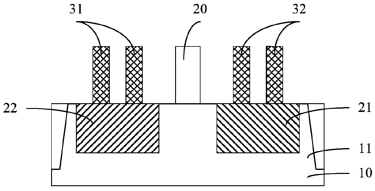
[0035] refer to figure 1 , shows a schematic diagram of the structure of a gated diode.

[0036] The gate control diode includes: a substrate 10, the surface of the substrate 10 has a fin 11, and a P-type well region is provided in the fin 11 and the substrate 10; a gate across the fin 11 20; the P-type doped region 21 and the N-type doped region 22 respectively located in the fins 11 on both sides of the gate 20; the first doped region across the fin 11 and respectively located on both sides of the gate 20 A conductive structure 31 and a second conductive structure 32, the first conductive structure 31 covers part of the sidewall and top surface of the N-type doped region 22, and the second ...


PUM


Abstract

The present invention provides a grid-controlled diode and a formation method thereof. The formation method comprises: providing a substrate, and forming a plurality of fin portions; forming a first control structure, wherein the first control structure comprises of a plurality of first grids crossing the fin portions, and the part of the side wall and the top portion of the fin portions are coated with the first grids; and forming a first doped region and a second doped region. The first control structure is arranged between the first doped region and the second doped region, the first control structure comprises a plurality of the first grids, and the size of the first control structure along the extension directions of the fin portions is larger than the size of a single first grid. The arrangement of the first control structure can effectively increase a distance between the first doped region and the second doped region to effectively prolong the length of the current channel of the grid-controlled diode and effectively expand the depth of the current channel of the grid-controlled diode so as to effectively improve the current jamming problem of the grid-controlled diode and improve the device performances.

Description

technical field [0001] The invention relates to the field of semiconductor manufacturing, in particular to a gate control diode and a forming method thereof. Background technique [0002] As semiconductor chips are used more and more widely, there are more and more factors that cause semiconductor chips to be damaged by static electricity. In the existing chip design, damage to the chip is often reduced by setting an electrostatic discharge (ESD, Electrostatic Discharge) protection structure in the chip. [0003] The design and application of existing electrostatic discharge protection circuits include: Gate Grounded NMOS (GGNMOS for short) protection circuit, shallow trench isolation structure diode (STI diode) protection circuit, gate control diode (Gated diode) Protection circuit, Laterally Diffused MOS (LDMOS for short) protection circuit, Bipolar Junction Transistor (BJT for short) protection circuit, etc. [0004] The existing electrostatic discharge protection struc...

Claims


Application Information

Patent Timeline
Patent Type & Authority Patents(China)
IPC IPC(8): H01L29/78H01L29/423H01L29/06H01L21/336H01L21/28
CPCH01L21/28H01L29/0603H01L29/4232H01L29/66795H01L29/785H01L29/7855
Inventor 甘正浩
Owner SEMICON MFG INT (SHANGHAI) CORP
Why Eureka
Try Eureka