Aluminum-gallium arsenide structure-based broadband perfect absorber
A gallium arsenide, wide-band technology, applied in the fields of optoelectronic materials and photonics, can solve the problems of poor repeatability of light absorption response, etc., and achieve the effects of simple structure, easy preparation, and wide application prospects
- Summary
- Abstract
- Description
- Claims
- Application Information
AI Technical Summary
Problems solved by technology
Method used
Image
Examples
Embodiment 1
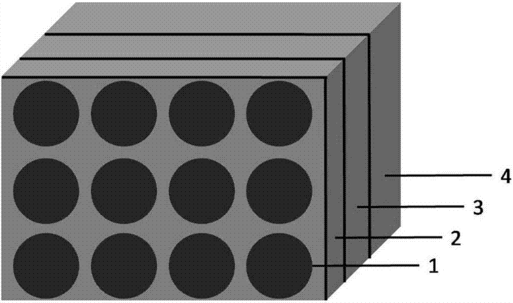
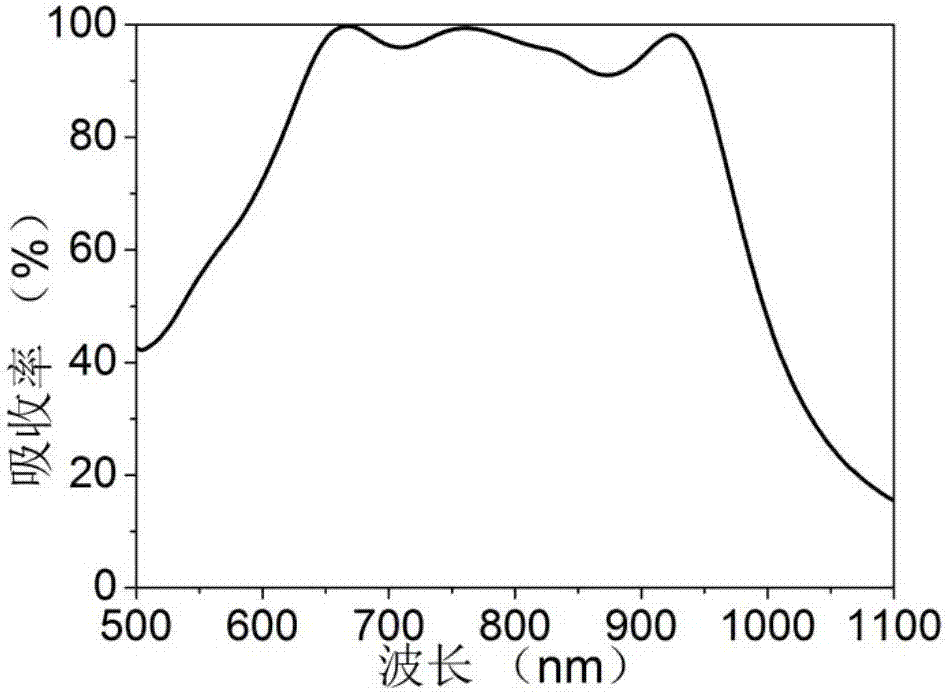
[0045] refer to figure 2 , figure 2 It is the light absorption diagram of the broadband light perfect absorber based on the aluminum-gallium arsenide structure in this embodiment. The thickness of the aluminum film layer is 100nm, and the thickness of the gallium arsenide film layer is 30nm. Gallium arsenide particles are cylindrical structures with a diameter of 380nm and a thickness of 30nm. The gallium arsenide grain array period size is 500nm. It can be seen from the figure that the maximum absorption rate reaches 99.8%, and the absorption rate in the spectral range from 615nm to 960nm exceeds 80%, indicating that the aluminum-gallium arsenide structure produces a wide-band light absorption response.
Embodiment 2
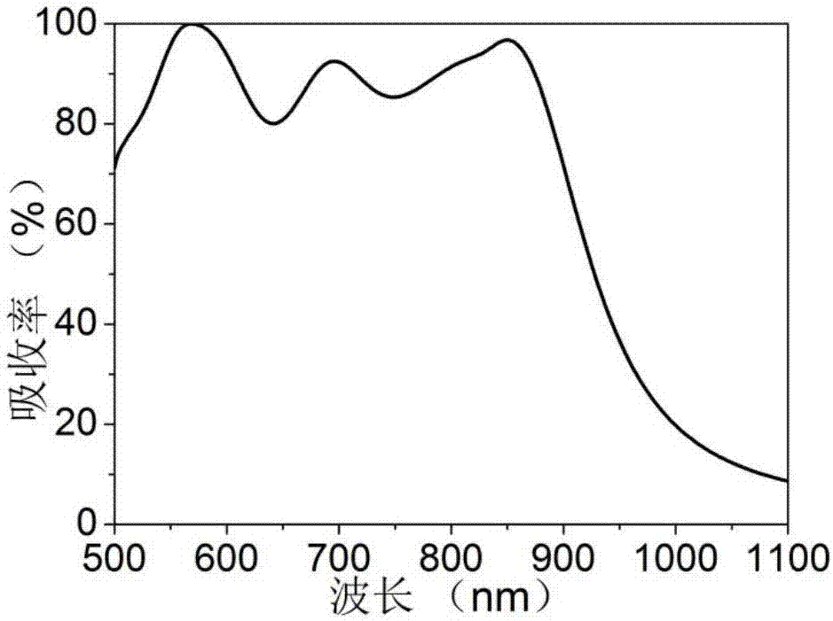
[0047] refer to image 3 , image 3 It is the light absorption diagram of the broadband light perfect absorber based on the aluminum-gallium arsenide structure in this embodiment. The thickness of the aluminum film layer is 100nm, and the thickness of the gallium arsenide film layer is 20nm. Gallium arsenide particles are cylindrical structures with a diameter of 380nm and a thickness of 30nm. The gallium arsenide grain array period size is 500nm. It can be seen from the figure that by adjusting the thickness of the gallium arsenide film layer in the absorber, the maximum absorption rate reaches 99.9%, and the absorption rate in the spectral range from 518nm to 888nm exceeds 80%, indicating that under this structural parameter, The Al-GaAs structure can also provide a broadband photoperfect absorption response.
Embodiment 3
[0049] refer to Figure 4 , Figure 4 It is the light absorption diagram of the broadband light perfect absorber based on the aluminum-gallium arsenide structure in this embodiment. The thickness of the aluminum film layer is 100nm, and the thickness of the gallium arsenide film layer is 40nm. Gallium arsenide particles are cylindrical structures with a diameter of 380nm and a thickness of 30nm. The gallium arsenide grain array period size is 500nm. It can be seen from the figure that by adjusting the thickness of the gallium arsenide film layer in the absorber, the size of the gallium arsenide grain and the size of the array period, the absorption rate in the spectral range from 702nm to 1010nm is more than 80%, indicating that in this structure Under the same parameters, the Al-GaAs structure can also provide a wide-band light perfect absorption response, and in addition, the maximum absorption rate reaches 96.5%.
PUM
| Property | Measurement | Unit |
|---|---|---|
| Thickness | aaaaa | aaaaa |
| Diameter | aaaaa | aaaaa |
| Thickness | aaaaa | aaaaa |
Abstract
Description
Claims
Application Information


