Organic light emitting diode display panel and manufacturing method thereof, and display device

A technology of light-emitting diodes and display panels, which is applied in the direction of organic semiconductor devices, semiconductor/solid-state device manufacturing, and electric solid-state devices. question

Active Publication Date: 2017-11-24
BOE TECH GRP CO LTD
View PDF7 Cites 10 Cited by
  • Summary
  • Abstract
  • Description
  • Claims
  • Application Information

AI Technical Summary

Problems solved by technology

Due to the free flow of droplets in the solution process, the flatness in the pixel has a great influence on the distribution of droplets. If the flatness of the flat layer is poor, it will further affect the thickness uniformity of the OLED film layer, resulting in uneven light emission of the pixels of the OLED device. The problem

Method used


Image

  • Organic light emitting diode display panel and manufacturing method thereof, and display device
  • Organic light emitting diode display panel and manufacturing method thereof, and display device
  • Organic light emitting diode display panel and manufacturing method thereof, and display device

Examples


Embodiment 1

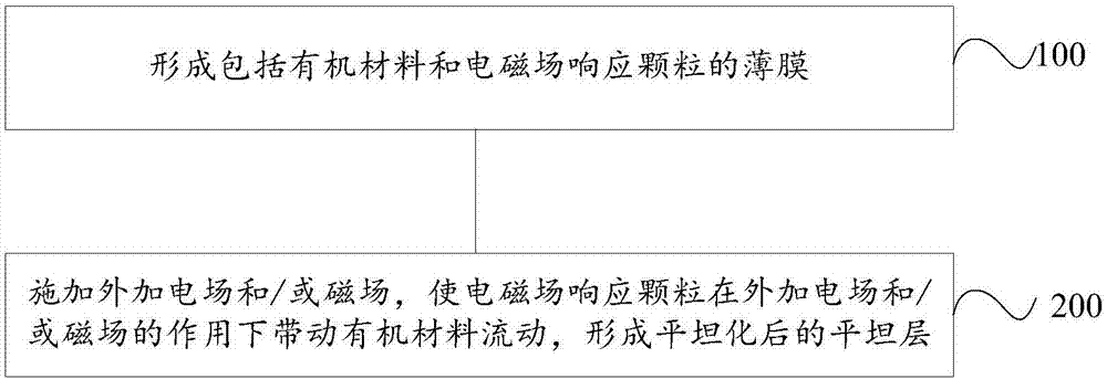
[0044] figure 1 The flow chart of the OLED display panel manufacturing method provided by Embodiment 1 of the present invention, as shown in figure 1 As shown, the OLED display panel manufacturing method provided by Embodiment 1 of the present invention specifically includes the following steps:

[0045] Step 100, forming a thin film including organic materials and electromagnetic field responsive particles.

[0046] Among them, the organic material is polymethyl methacrylate, polyimide, silicone material, etc., and the electromagnetic field responsive particle is a particle that can respond to both an electric field and a magnetic field, and has a nanometer-scale diameter. It should be noted that the response to an electric field Specifically, it means that particles can move under the action of an electric field. Similarly, responding to a magnetic field means that particles can move under the action of a magnetic field.

[0047] Specifically, the electric field responsive...

Embodiment 2

[0074] Based on the above inventive concept, Embodiment 2 of the present invention provides another OLED display panel manufacturing method, which is different from the OLED display panel manufacturing method provided in Embodiment 1 of the present invention in that:

[0075] Step 100 specifically includes: coating a thin film comprising an organic material on the thin film transistor; and doping the organic material with electromagnetic field responsive particles.

[0076] Specifically, the thin film transistor in this embodiment has a top-gate structure, which includes: an active layer, a gate insulating layer disposed on the active layer and covering the entire substrate, a gate electrode disposed on the gate insulating layer, and a gate electrode disposed on the gate An interlayer insulating layer on the electrodes and covering the entire substrate, and a source-drain electrode arranged on the interlayer insulating layer and electrically connected to the active layer.

[0...

Embodiment 3

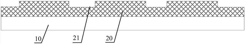
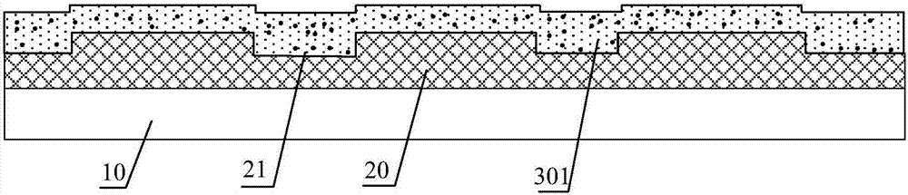
[0101] Based on the inventive concepts of the foregoing embodiments, Figure 4 A schematic structural diagram of the OLED display panel provided in Embodiment 3 of the present invention, as shown in Figure 4 As shown, the OLED display panel provided by the embodiment of the present invention is manufactured by using the OLED display panel manufacturing method of Embodiment 1 or Embodiment 2, and its realization principle and effect are similar, and will not be repeated here.

[0102] Specifically, the OLED display panel provided in this embodiment includes: a substrate 10 , a thin film transistor 20 with a plurality of recessed regions 21 disposed on the upper surface of the substrate 10 , and a flat layer 30 disposed on the side of the thin film transistor 20 away from the substrate 10 .


PUM


Abstract

The embodiment of the invention discloses an organic light emitting diode display panel and a manufacturing method thereof, and a display device. The method comprises: forming a thin film comprising organic materials and electromagnetic field response particles; and applying and applied electric field and/or magnetic field to allow the electromagnetic field response particles to drive the flow of the organic materials under the action of the applied electric field and/or the magnetic field to form a flat layer after planarization. According to the embodiment of the invention, the electromagnetic field response particles are added to allow the electromagnetic field response particles to be moved under the action of the applied electric field and/or the magnetic field and drive the movement of the organic materials with the movement of the electromagnetic field response particles so as to realize planarization of the flat layer, allow the OLED film layer manufactured on the flat layer to be more uniform and improve the luminescence uniformity in the pixels in the OLED device.

Description

technical field [0001] The invention relates to the field of display technology, in particular to an organic light emitting diode display panel, a manufacturing method thereof, and a display device. Background technique [0002] In the field of display, compared with Liquid Crystal Display (LCD), Organic Light-Emitting Diode (OLED) has the advantages of self-illumination, fast response, wide viewing angle, high brightness, bright color, and thinness. [0003] According to different ways of coupling out light, OLED devices can be divided into top-emitting OLED devices and bottom-emitting OLED devices. In a top-emitting OLED device, in order to fabricate an OLED device functional layer on a thin film transistor (Thin Film Transistor, TFT for short) and ensure the flatness of the functional layer, it is necessary to fabricate a flat layer on the TFT. [0004] The existing methods of film formation of OLED devices mainly include evaporation process and solution process. Among t...

Claims


Application Information

Patent Timeline
Patent Type & Authority Applications(China)
IPC IPC(8): H01L51/56H01L51/50H01L27/32
CPCH10K71/10H10K71/191H10K59/12H10K50/00H10K59/124H10K2102/331H10K71/00H10K71/135H10K59/90
Inventor 侯文军
Owner BOE TECH GRP CO LTD
Why Eureka
Try Eureka