Off-chip capacitor-less LDO circuit based on through silicon via array
A technology without off-chip capacitors and through-silicon vias. It can be used in the fields of adjusting electrical variables, control/regulating systems, and instruments. It can solve problems such as high static power consumption overhead, and achieve improved loop stability, noise suppression, and power supply suppression. high effect
- Summary
- Abstract
- Description
- Claims
- Application Information
AI Technical Summary
Problems solved by technology
Method used
Image
Examples
Embodiment 1
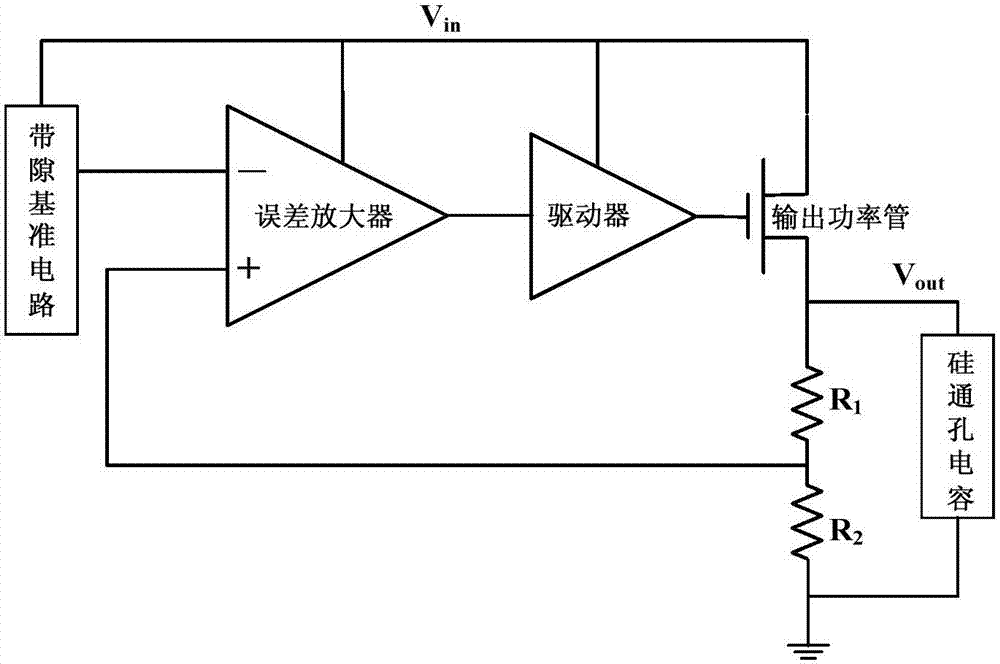
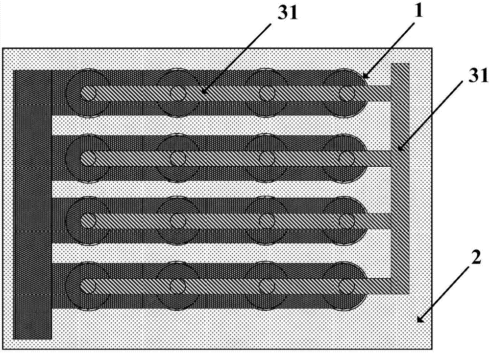
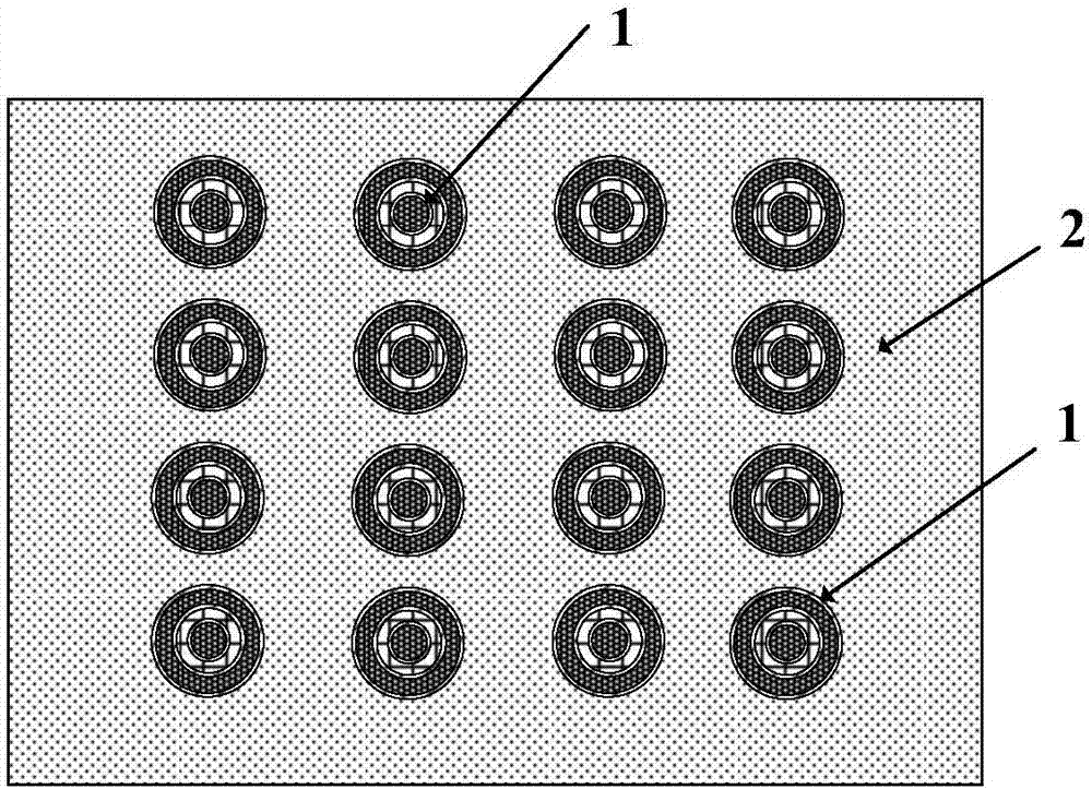
[0018] The non-external capacitor LDO circuit based on the TSV array of embodiment 1, such as Figure 1 ~ Figure 4 As shown, it includes a bandgap reference circuit, an error amplifier, a driver, an output power tube, a sampling resistor network, and a TSV capacitor. The positive input of the error amplifier is connected to the output of the sampling resistor network, and the negative input of the error amplifier is connected to the band The output terminal of the gap reference circuit is connected, the output terminal of the error amplifier is connected to the input terminal of the driver, the output terminal of the driver drives the output power transistor, and the output terminal of the output power transistor is respectively connected to one end of the sampling resistor network and one end of the TSV capacitor , the other end of the sampling resistor network is connected to the other end of the TSV capacitor and grounded, and the bandgap reference circuit, error amplifier, ...
Embodiment 2
[0025] The LDO circuit without external capacitors based on the TSV array in Embodiment 2 has the same structure as that of the LDO circuit in Embodiment 1, except that in Embodiment 2, the TSV capacitance consists of 50×50 coaxial silicon through-hole configuration. The AC characteristic curve of the LDO circuit of embodiment 2 is shown in Figure 5 . From Figure 5 From the AC characteristic curve shown, it can be seen that the DC gain of the LDO circuit is 66.13dB, the phase margin is 86.3 degrees, and the gain margin is -49.3 degrees. The entire LDO circuit can work stably. The power supply rejection ratio characteristic curve of the LDO circuit of embodiment 2 sees Figure 6 . From Figure 6 It can be seen from the power supply rejection ratio characteristic curve shown that the full frequency band power supply rejection ratio of the LDO circuit is greater than -72.5dB, which can effectively suppress the noise introduced by the input power supply.
[0026] The prese...
PUM
 Abstract
Description
Claims
Application Information


