Electronic circuit package using composite magnetic sealing material

A technology for electronic circuits and magnetic fillers, applied in circuits, electrical components, electrical solid devices, etc., can solve problems such as interface peeling of mold materials, cracks in electronic components or mold materials, and achieve the effect of preventing warpage

Active Publication Date: 2017-12-01
TDK CORPARATION
View PDF6 Cites 6 Cited by
  • Summary
  • Abstract
  • Description
  • Claims
  • Application Information

AI Technical Summary

Problems solved by technology

[0007] On the other hand, since the difference in physical properties between the semiconductor IC and electronic components mounted on the substrate and the mold material also generates stress, various problems such as interface peeling of the mold material and cracks of the electronic component or mold material may occur. question

Method used


Image

  • Electronic circuit package using composite magnetic sealing material
  • Electronic circuit package using composite magnetic sealing material
  • Electronic circuit package using composite magnetic sealing material

Examples


no. 1 Embodiment approach >

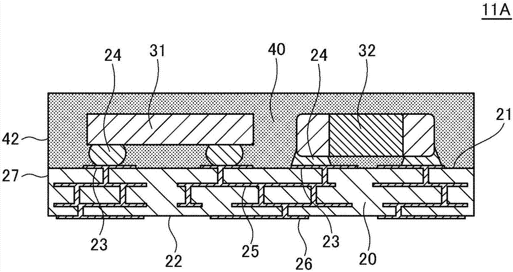
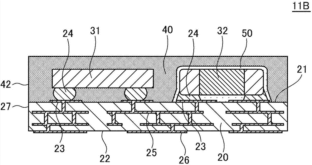
[0065] figure 1 It is a sectional view showing the structure of the electronic circuit package 11A according to the first embodiment of the present invention.

[0066] Such as figure 1 As shown, the electronic circuit package 11A according to the present embodiment includes a substrate 20 , a plurality of electronic components 31 and 32 mounted on the substrate 20 , and a magnetic mold covering the surface 21 of the substrate 20 to embed the electronic components 31 and 32 . Resin 40.

[0067] The type of electronic circuit package 11A involved in this embodiment is not particularly limited, and examples include high-frequency modules that process high-frequency signals, power modules that perform power control, and system-in-packages that have a 2.5D structure or a 3D structure. (SIP: system in package), semiconductor packages for wireless communication or digital circuits, etc. exist figure 1 Only two electronic components 31 and 32 are shown in , but actually a pluralit...

no. 2 Embodiment approach >

[0109] Figure 15 It is a cross-sectional view showing the structure of an electronic circuit package 12A according to the second embodiment of the present invention.

[0110] Such as Figure 15 As shown, in the electronic circuit package 12A according to this embodiment, the planar size of the magnetic molding resin 40 is only slightly smaller than the planar size of the substrate 20 , and thus the outer peripheral portion of the surface 21 of the substrate 20 is exposed from the magnetic molding resin 40 . and figure 1 The electronic circuit package 11A according to the first embodiment shown is different. Since other configurations are the same as those of the electronic circuit package 11A according to the first embodiment, the same reference numerals are assigned to the same elements, and overlapping descriptions are omitted.

[0111] In the electronic circuit package 12A according to the present embodiment, as illustrated, in the present invention, the side surface 42...

no. 3 Embodiment approach >

[0117] Figure 19 It is a cross-sectional view showing the structure of an electronic circuit package 13A according to the third embodiment of the present invention.

[0118] Such as Figure 19 As shown, the electronic circuit package 13A according to this embodiment is further equipped with the metal film 60 covering the upper surface 41 and the side surface 42 of the magnetic molding resin 40 and the side surface 27 of the substrate 20 . figure 1 The electronic circuit package 11A according to the first embodiment shown is different. In addition, among the internal wiring 25 , the internal wiring 25 with a G at the end of the symbol is a power supply pattern, and a part of it is exposed on the side surface 27 of the substrate 20 . The power supply pattern 25G is typically a ground pattern that provides a ground potential, but is not limited to a ground pattern as long as it is a line pattern that provides a fixed potential. Since other configurations are the same as those...


PUM

PropertyMeasurementUnit
thicknessaaaaaaaaaa
electrical resistivityaaaaaaaaaa
particle diameteraaaaaaaaaa

Abstract

The invention provides an electronic circuit package using a composite magnetic sealing material as a mold material. Disclosed herein is an electronic circuit package includes a substrate, an electronic component mounted on a surface of the substrate, and a magnetic mold resin covering the surface of the substrate so as to embed therein the electronic component. The magnetic mold resin includes a resin material and a filler blended in the resin material in a blended ratio of 30 vol. % or more to 85 vol. % or less. The filler includes a magnetic filler containing Fe and 32 wt. % or more and 39 wt. % or less of a metal material contained mainly of Ni, thereby a thermal expansion coefficient of the magnetic mold resin is 15 ppm/ DEG C. or less.

Description

technical field [0001] The present invention relates to an electronic circuit package, and more particularly to an electronic circuit package using a composite magnetic sealing material as a molding material. Background technique [0002] In recent years, electronic devices such as smartphones have tended to adopt high-performance radio communication circuits and digital chips, and the operating frequency of semiconductor ICs used is also increasing. In addition, the system-in-package (SIP: system in package) with a 2.5D structure or a 3D structure that connects multiple semiconductor ICs with the shortest wiring is accelerating, and it can be predicted that the modularization of power supply system circuits will continue to increase in the future. . In addition, multiple electronic components can be predicted (passive components such as inductors, capacitors, resistors, and filters; active components such as transistors and diodes; integrated circuit components such as sem...

Claims


Application Information

Patent Timeline
Patent Type & Authority Applications(China)
IPC IPC(8): H01L23/29H01L23/552
CPCH01L23/295H01L23/552H01L2224/16225H01L2224/97H01L2924/15313H01L2924/181H01L2924/19105H01L2924/3025H01L2924/00012H01L2224/81
Inventor 川畑贤一
Owner TDK CORPARATION
Why Eureka
Try Eureka