
Charge transfer type analog count reading circuit based on pulse rising edge triggering

A readout circuit and charge transfer technology, which is applied to the pulse counter of optoelectronic devices, the pulse counter of semiconductor devices with only two electrodes, and pulse technology, etc. problems such as poor degree of accuracy and poor uniformity of counting step length, to achieve the effect of simple circuit, high counting range and good performance consistency

Active Publication Date: 2017-12-01
NANJING UNIV OF POSTS & TELECOMM
View PDF11 Cites 7 Cited by
  • Summary
  • Abstract
  • Description
  • Claims
  • Application Information

AI Technical Summary

Problems solved by technology

The simple analog counting circuit proposed earlier is sensitive to the pulse width of the input avalanche pulse, requires a large integral capacitor, and the uniformity of the counting step is poor
Later, an analog counting circuit based on charge sharing was proposed. Although the uniformity between different pixel units was improved, the linearity of the counting step was poor.
In order to solve the problem of poor linearity, a level-triggered charge-transfer analog counting circuit is proposed, but an integration capacitor of 350fF is still required to achieve an 8-bit counting resolution. If a higher bit resolution is achieved, the counting circuit area is still large

Method used


Image

  • Charge transfer type analog count reading circuit based on pulse rising edge triggering
  • Charge transfer type analog count reading circuit based on pulse rising edge triggering
  • Charge transfer type analog count reading circuit based on pulse rising edge triggering

Examples


specific Embodiment

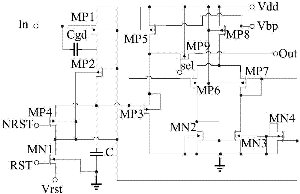
[0022] Such as figure 1 As shown, the parameters of the MOSFET transistor and the integral capacitor in the analog counting readout circuit proposed by the present invention are set as follows: the length and the width of the input tube MP1 grid are 300nm; the length and the width of the charge transfer tube MP2 grid are respectively 2 μm and 300nm, the length and width of the gate of the source follower transistor MP3 are 300nm and 12μm respectively, and the length and width of the gate of the reset PMOS transistor MP4 are 300nm and 1μm respectively. Both MP5 and MP8 are used as current source loads, and the length and width of their gates are both 1 μm. MP6 and MP7 are used as unit gain amplifier input tubes, the length and width of the grid are 1 μm and 2 μm respectively, and the length and width of the grid of the row selection transistor MP9 are both 300 nm. The length and width of the gate of the reset NMOS transistor MN1 are 350nm and 440nm respectively, and the length...


PUM


Abstract

The invention discloses a charge transfer type analog count reading circuit based on pulse rising edge triggering. The circuit comprises 13 MOSFET transistors, an integral capacitor and a parasitic capacitor. The MP1 and MP2 are a charge injection switch and a charge transfer switch and are used for controlling generation and transfer of a charge packet. The parasitic capacitor Cgd bridged between a gate and a drain of the MP1 couples an input avalanche pulse signal into the drain of the MP1. The MP4 and MN1 form a reset circuit which is used for discharging charges stored by the integral capacitor. The MP6, MP7, MP8, MN2, MN3 and MN4 form a unit gain amplifier which is used for preventing a voltage of the integral capacitor from being influenced by electric leakage of the MOSFET transistor connected with the integral capacitor C. The MP3 is a source follower transistor. The MP5 is a load. The MP9 is a lien selection transistor. The voltage on the integral capacitor C is read to an external circuit through the MP3 and the MP9. According to the analog count reading circuit, a wide count range can be realized, moreover, an area of SPAD array detector pixel units can be reduced, and the density of an SPAD array detector is improved.

Description

technical field [0001] The invention relates to a charge-transfer type analog counting readout circuit triggered by pulse rising edge, which belongs to the field of optoelectronic technology. Background technique [0002] Single-photon avalanche diode (SPAD) has been widely used in bioluminescent lifetime imaging, Raman spectroscopy, 3D imaging and other technical fields due to its high sensitivity and sub-second time resolution. At present, single-photon avalanche diodes are developing towards low-cost, high-density, high-reliability deep submicron CMOS process array image sensors. A SPAD array detector includes numerous SPAD pixel units and peripheral readout and control circuits. In order to increase the density of the SPAD array detector, the area of ​​the SPAD pixel unit must be reduced. Each SPAD pixel unit is composed of a SPAD device, a quenching reset circuit and a counting readout circuit. Traditional counting circuits all use digital counting circuits, which hav...

Claims


Application Information

Patent Timeline
Patent Type & Authority Applications(China)
IPC IPC(8): H03K21/08H03K23/78H03K23/80
CPCH03K21/08H03K23/78H03K23/80
Inventor 徐跃李鼎赵庭晨
Owner NANJING UNIV OF POSTS & TELECOMM
Learn More