Film thickness measuring method, film thickness measuring device, polishing method, and polishing device

A measurement method and film thickness technology, which is applied in the direction of grinding equipment, measuring equipment, grinding machine tools, etc., can solve the problem of easily changing peak value

Active Publication Date: 2017-12-01
EBARA CORP
View PDF9 Cites 5 Cited by
  • Summary
  • Abstract
  • Description
  • Claims
  • Application Information

AI Technical Summary

Problems solved by technology

Especially when measuring the film thickness while polishing the wafer, since the wafer and the film thickness s

Method used


Image

  • Film thickness measuring method, film thickness measuring device, polishing method, and polishing device
  • Film thickness measuring method, film thickness measuring device, polishing method, and polishing device
  • Film thickness measuring method, film thickness measuring device, polishing method, and polishing device

Examples


Embodiment Construction

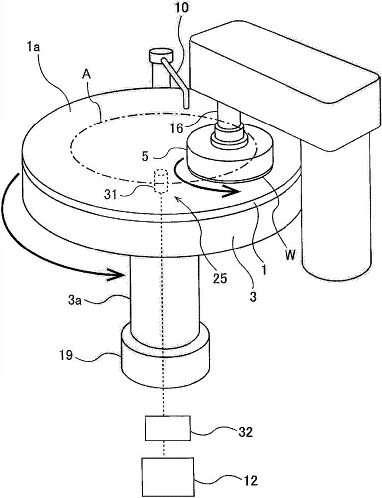
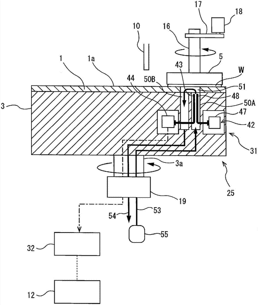
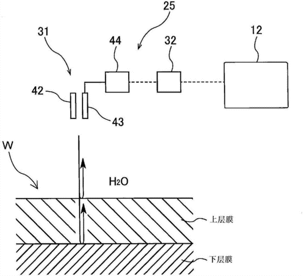
[0063] Hereinafter, embodiments of the present invention will be described with reference to the drawings. figure 1 It is a figure which shows the grinding|polishing apparatus which is one embodiment of this invention. Such as figure 1 As shown, the polishing apparatus includes: a polishing table 3 on which a polishing pad 1 having a polishing surface 1 a is installed; a wafer W for holding an example of a substrate, and polishing while pressing the wafer W against the polishing pad 1 on the polishing table 3 A polishing head 5; a polishing liquid supply nozzle 10 for supplying a polishing liquid (such as slurry) on the polishing pad 1; and a polishing control unit 12 for controlling the polishing of the wafer W.

[0064] The grinding table 3 is connected to a table motor 19 disposed below it via a table shaft 3 a, and the grinding table 3 is rotatable in the direction indicated by the arrow by the table motor 19 . A polishing pad 1 is attached to the upper surface of the ...


PUM


Abstract

The present invention relates to a film thickness measuring method that detects a film thickness by analyzing optical information contained in light reflected from a substrate. The film thickness measuring method includes the steps of generating a spectral waveform showing the relationship between the strength and wavelength of the reflected light from the substrate (W), determining the intensity of the frequency component and corresponding film thickness by performing a Fourier transformation process on the spectral waveform, determining the plurality of maximal values (M1, M2) of the intensity of the frequency component, and selecting one film thickness according to a selection standard from film thicknesses (t1, t2) corresponding respectively to the maximal values (M1, M2). The selection standard is either selecting the Nth largest film thickness or selecting the Nth smallest film thickness, wherein N is a natural number defined beforehand.

Description

technical field [0001] The present invention relates to a film thickness measurement method and a film thickness measurement device of a substrate (such as a wafer) on which a film is formed, and more particularly to a film thickness measurement that detects the film thickness by analyzing optical information included in reflected light from the substrate Method and film thickness measuring device. Furthermore, the present invention relates to a polishing method and a polishing apparatus using such a film thickness measuring method and film thickness measuring device. Background technique [0002] The manufacturing process of semiconductor devices includes various processes such as the process of polishing insulating films such as SiO2, and the process of polishing metal films such as copper and tungsten. The manufacturing process of back-illuminated CMOS (complementary metal oxide semiconductor) sensors and through-silicon vias (TSV: Through-Silicon Via) includes the proce...

Claims


Application Information

Patent Timeline
IPC IPC(8): G01B11/06B24B37/013B24B49/04B24B49/12H01L21/304
CPCB24B37/013B24B37/107B24B37/205B24B49/12G01B11/0625G01B11/0683H01L22/12H01L22/26B24B49/04G01B11/06H01L21/304
Inventor 金马利文
Owner EBARA CORP
Why Eureka
Try Eureka