
Avalanche photodiode and method of manufacturing the same

A technology of avalanche optoelectronics and manufacturing methods, which is applied in the direction of circuits, electrical components, semiconductor devices, etc., can solve the problems of edge effect, photosensitive area limitation, leakage of avalanche photodiodes, etc., and achieve low dark current reduction, high signal-to-noise ratio, and Effect of reducing edge leakage

Active Publication Date: 2019-07-26
BYD SEMICON CO LTD
View PDF3 Cites 0 Cited by
  • Summary
  • Abstract
  • Description
  • Claims
  • Application Information

AI Technical Summary

Problems solved by technology

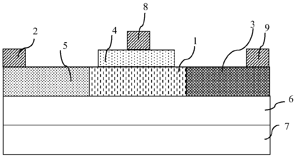
[0003] The above-mentioned avalanche photodiode belongs to the lateral structure, that is, the diode structure formed by the P-type doped region 5 and the N-type doped region 3 is lateral, and the area of ​​the photosensitive region 4 is also smaller than the avalanche region 1, and the avalanche region 1 is determined according to the operating voltage. Certainly, under a certain working voltage and avalanche gain conditions, the width of the avalanche area 1 is basically fixed, making the size of the photosensitive area 4 not flexible enough, and the photosensitive area is limited
In addition, neither the P-type doped region 5 nor the N-type doped region 3 can form a closed loop on the photosensitive region 4, and there is an edge effect, which leads to leakage of the avalanche photodiode

Method used


Image

  • Avalanche photodiode and method of manufacturing the same
  • Avalanche photodiode and method of manufacturing the same
  • Avalanche photodiode and method of manufacturing the same

Examples


Embodiment Construction

[0022] Embodiments of the present invention are described in detail below, examples of which are shown in the drawings, wherein the same or similar reference numerals designate the same or similar elements or elements having the same or similar functions throughout. The embodiments described below by referring to the figures are exemplary only for explaining the present invention and should not be construed as limiting the present invention.

[0023] In describing the present invention, it should be understood that the terms "longitudinal", "transverse", "upper", "lower", "front", "rear", "left", "right", "vertical", The orientation or positional relationship indicated by "horizontal", "top", "bottom", "inner", "outer", "front", "back", etc. are based on the orientation or positional relationship shown in the attached drawings, and are only for the convenience of description The present invention and simplified description do not indicate or imply that the device or element re...


PUM


Abstract

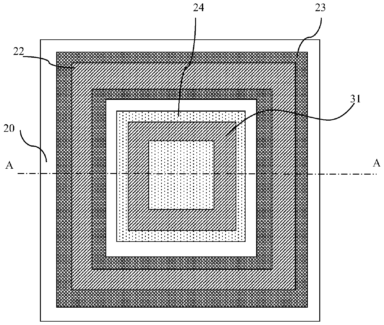
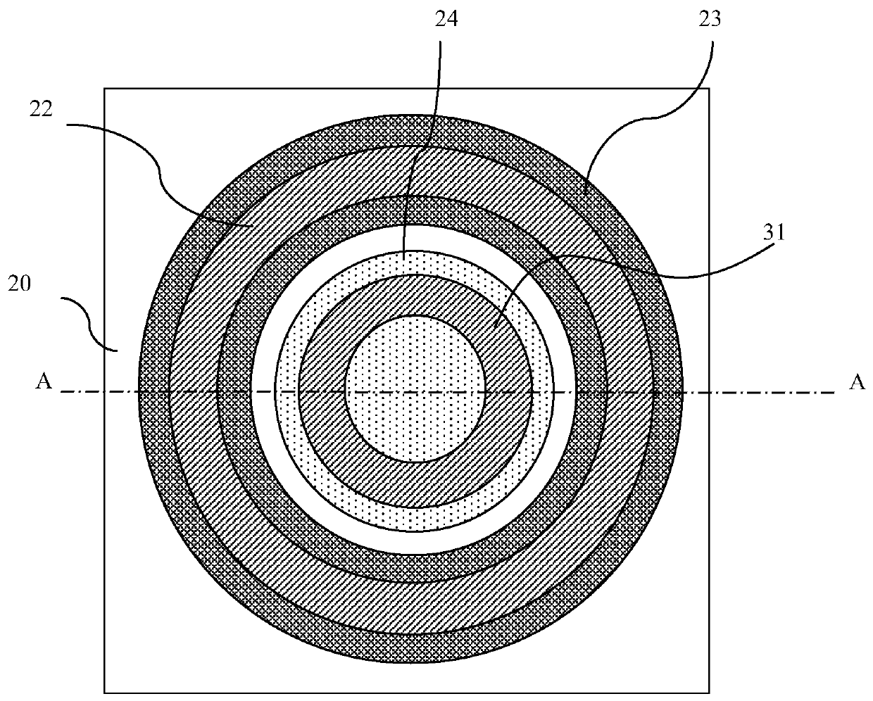
The invention proposes an avalanche photodiode and a manufacturing method thereof. A light-sensitive region of the avalanche photodiode is completely isolated with a first conductive type of doping region and a second conductive type of doping region, the light-sensitive area is free from the influence of a working voltage and avalanche gain, and the light-sensitive area is encircled by the first conductive type of doping region and the second conductive type of doing region. By the avalanche photodiode, the edge electric leakage can be effectively reduced, and the avalanche photodiode is low in dark current and high in signal-to-noise ratio.

Description

technical field [0001] The invention belongs to the field of basic electrical components, and relates to semiconductor devices, in particular to an avalanche photodiode and a manufacturing method thereof. Background technique [0002] figure 1 It is an existing avalanche photodiode, including: a silicon substrate 7, an oxide layer 6 grown above the silicon substrate 7, the oxide layer 6 and the silicon substrate 7 are bonded to the silicon material device layer, and the silicon material device layer is formed There are P-type doped region 5, N-type doped region 3 and avalanche gain region 1, wherein avalanche gain region 1 is sandwiched between P-type doped region 5 and N-type doped region 3, and photosensitive region 4 is located in the avalanche gain region 1, the photosensitive region 4 is in contact with the avalanche gain region 1 but not in contact with the P-type doped region 5 and the N-type doped region 3, the surface of the P-type doped region 5 is connected to th...

Claims


Application Information

Patent Timeline
Patent Type & Authority Patents(China)
IPC IPC(8): H01L31/0352H01L31/107H01L31/18
CPCH01L31/03529H01L31/107H01L31/1804
Inventor 刘东庆
Owner BYD SEMICON CO LTD
Learn More