A kind of solar cell preparation method

A technology for solar cells and silicon wafers, which is applied to circuits, electrical components, and final product manufacturing. The effect of edge leakage, reduction of silicon dangling bonds, and improvement of short-circuit current density

Active Publication Date: 2016-01-13
山东力诺阳光电力科技有限公司
View PDF4 Cites 0 Cited by
  • Summary
  • Abstract
  • Description
  • Claims
  • Application Information

AI Technical Summary

Problems solved by technology

[0004] At present, the emitter made by the conventional diffusion method cannot meet the above two requirements at the same time
Generally, if the doping concentration is not too high, the Auger recombination will be greatly increased, and the minority carriers formed in the emission region are easy to recombine, resulting in a decrease in short-wave response; if the surface concentration is reduced, the junction depth will also become shallower, thin layer The resistance is high, and the resistance of the emitter must increase, thereby increasing the resistance of the current moving to the grid electrode in the emission area, increasing the probability of PN junction burn-through in the subsequent electrode sintering process, and reducing the battery yield.

Method used


Image

  • A kind of solar cell preparation method
  • A kind of solar cell preparation method

Examples


Embodiment 1

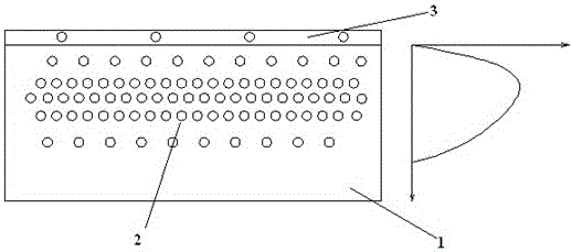
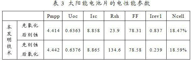
[0022] Select a single crystal silicon wafer; silicon wafer 1 undergoes a conventional cleaning process and texturing, puts silicon wafer 1 into a diffusion furnace, heats up to 810°C, and feeds large nitrogen (8L / min), small nitrogen (1.7L / min), oxygen (1L / min) for 12min, and after the temperature rises to 855°C, the diffusion junction advances for 7min; the diffused silicon wafer 1 is placed in 2% hydrofluoric acid, and the reaction time is 90s; the obtained silicon wafer 1 is placed again Put into the oxidation furnace, feed large nitrogen (7L / min), oxygen (1L / min), keep the temperature at 870°C for 5min; adopt PECVD process to make a silicon nitride film on the surface of silicon wafer 1 with a thickness of 85nm and a refractive index of 85nm. The ratio is 2.08; and then screen printing and sintering are used in sequence to obtain finished solar cells. Comparing the battery sheet obtained in Example 1 of the present invention with the battery sheet of the prior art, the r...

Embodiment 2

[0025] Select a quasi-single crystal silicon wafer; silicon wafer 1 undergoes a conventional cleaning process and texturing, puts silicon wafer 1 into a diffusion furnace, heats up to 785°C, and feeds large nitrogen (6.5L / min), small nitrogen (1L / min), oxygen (0.25L / min) diffused for 15min, and after the temperature was raised to 830°C, the diffusion junction was advanced for 15min; the diffused silicon wafer 1 was placed in 5% hydrofluoric acid, and the reaction time was 50s; the obtained silicon wafer 1 Put it into the oxidation furnace again, feed large nitrogen (7L / min), oxygen (0.25L / min), keep the temperature at 820°C, and the time is 10min; adopt the PECVD process to make a silicon nitride film on the surface of the silicon wafer 1. The thickness of the film is 75nm, and the refractive index is 2.13; then screen printing and sintering are used in sequence to obtain finished solar cells. Comparing the battery sheet obtained in Example 2 of the present invention with the...

Embodiment 3

[0028] Select single crystal silicon wafer; silicon wafer 1 undergoes conventional cleaning process and texturing, diffusion process: put the silicon wafer into a diffusion furnace, heat up to 800°C, and feed large nitrogen (7L / min), small nitrogen (1.5 L / min), oxygen (0.9L / min) to diffuse for 10 minutes, after the temperature rises to 845°C, the diffusion junction advances for 10 minutes; etching process: silicon wafer 1 is placed in 7% hydrofluoric acid, and the reaction time is 30s; oxidation process : put into the oxidation furnace, feed large nitrogen (7L / min), oxygen (0.6L / min), keep the temperature at 870°C, and the time is 8min; adopt the PECVD process to make a silicon nitride film on the surface of the silicon wafer 1 with a thickness of 80nm, the refractive index is 2.10; and then screen printing and sintering are used in sequence to obtain finished solar cells. Comparing the battery sheet obtained in Example 3 of the present invention with oxidation first and then ...


PUM


Abstract

The invention relates to a method for preparing a solar cell. It specifically has the following steps: 1) Make an emitter on the surface of the silicon wafer after texturing; 2) Use HF acid solution to remove the phosphosilicate glass from the silicon wafer obtained in step 1; 3) Make carbon dioxide on the surface of the silicon wafer obtained in step 2 Silicon layer; 4) The silicon wafer obtained in step 3 is etched on the periphery, deposited silicon nitride film, screen-printed front and back electrodes and back aluminum, and sintered. It can effectively improve the uniformity of diffusion resistance and increase the lifetime of minority carriers; in addition, the passivation of silicon oxide reduces the dangling bonds of silicon and reduces the surface state, which can increase the short-circuit current density by 0.1-1mA / cm2, and the open-circuit voltage Increase by 3-10mV, and increase conversion efficiency by 0.1-0.5%. Edge etching after making silicon oxide can effectively reduce edge leakage and increase the parallel resistance of the battery.

Description

technical field [0001] The invention relates to the technical field of solar cell manufacturing, in particular to a solar cell manufacturing method. Background technique [0002] Among all kinds of solar cells, crystalline silicon cells have always occupied the most important position. In recent years, great achievements and progress have been made in improving efficiency and reducing cost of crystalline silicon solar cells, further enhancing its dominant position in the future photovoltaic industry. [0003] As the core component of the solar cell, the emitter's surface doping concentration will directly affect the conversion efficiency of the solar cell. Solar cells have two requirements for the emitter: 1. The doping concentration should not be too high, and 2. The surface concentration should not be too low. [0004] At present, the emitter made by the conventional diffusion method cannot meet the above two requirements at the same time. Generally, if the doping conce...

Claims


Application Information

Patent Timeline
Patent Type & Authority Patents(China)
IPC IPC(8): H01L31/18
CPCY02P70/50
Inventor 任现坤李秉霖姜言森张春艳程亮贾河顺徐振华
Owner 山东力诺阳光电力科技有限公司
Why Eureka
Try Eureka