Fingerprint recognition device, array substrate and display device

A fingerprint recognition and array substrate technology, which is applied in character and pattern recognition, acquisition/organization of fingerprints/palmprints, instruments, etc., and can solve problems such as difficulty in fingerprint recognition.

Active Publication Date: 2017-12-12
BOE TECH GRP CO LTD
View PDF3 Cites 6 Cited by
  • Summary
  • Abstract
  • Description
  • Claims
  • Application Information

AI Technical Summary

Problems solved by technology

[0005] The present invention provides a fingerprint identification device, an array substrate and a display device to solve the problem of difficulty in fingerprint identification of existing optical fingerprint identification devices

Method used


Image

  • Fingerprint recognition device, array substrate and display device
  • Fingerprint recognition device, array substrate and display device
  • Fingerprint recognition device, array substrate and display device

Examples


Embodiment 1

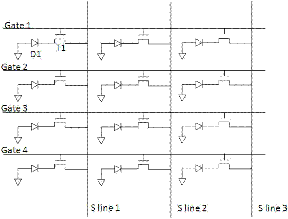
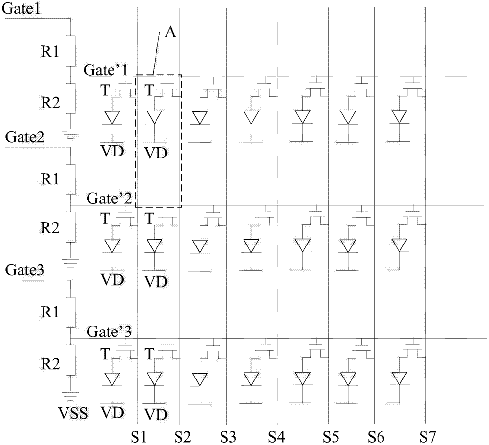
[0032] refer to figure 2 , shows the circuit principle structure diagram of the fingerprint identification device of the present invention.

[0033] An embodiment of the present invention provides a fingerprint identification device, including a first gate line, a second gate line, a reading signal line, and a voltage dividing unit. The intersection of the second gate line and the reading signal line defines a plurality of fingerprints. An identification unit A, the fingerprint identification unit A includes a photosensitive device VD and a thin film transistor T;

[0034] The first gate line is connected to the voltage dividing unit, and the voltage dividing unit includes a pressure sensitive device and an equivalent resistance connected in series, and the second gate line is connected between the pressure sensitive device and the equivalent resistance between.

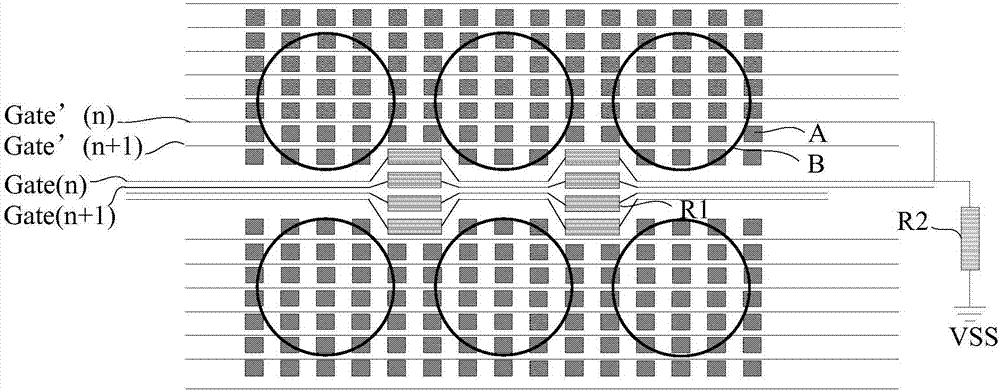
[0035] Such as figure 2 As shown, the first gate lines include Gate1, Gate2, and Gate3, the second gate lines...

Embodiment 2

[0069] Embodiment 2 of the present invention provides an array substrate, including the above-mentioned fingerprint identification device, the fingerprint identification device includes a first grid line, a second grid line, a reading signal line, and a voltage dividing unit, and the second grid line and The reading signal lines cross to define a plurality of fingerprint identification units, the fingerprint identification units include photosensitive devices and thin film transistors; the first gate line is connected to the voltage dividing unit, and the voltage dividing unit includes pressure sensitive A device and an equivalent resistance, the second gate line is connected between the pressure sensitive device and the equivalent resistance.

[0070] Wherein, when the thin film transistor is an N-type thin film transistor, when the voltage sensitive device is not pressed, the gate voltage of the thin film transistor is lower than the critical turn-on voltage. When the thin f...

Embodiment 3

[0079] Embodiment 3 of the present invention also provides a display device, including a light emitting unit, a light guide plate, a small hole plate, and the above-mentioned array substrate.

[0080] refer to Figure 7 , shows a schematic structural view of the display device of the present invention.

[0081] Among them, 71 is a fingerprint of a finger, 72 is a light emitting unit, 73 is a light guide plate, 74 is a small hole plate, 75 is an array substrate, and a plurality of small holes 741 are distributed on the small hole plate 74, and the array substrate 75 is provided with The fingerprint recognition device, the fingerprint recognition device includes a pressure sensitive device 751 and a photosensitive device 752 .

[0082] It should be noted that the fingerprint identification device also includes an equivalent resistance and a thin film transistor (not shown in the figure); Figure 7 The photosensitive device 752 in is not a photosensitive device, but a photosens...


PUM


Abstract

The invention provides a fingerprint recognition device, an array substrate and a display device and relates to the field of display technology. The fingerprint recognition device comprises first gate lines, second gate lines, reading signal lines and pressure splitting units, wherein the second gate lines and the reading signal lines intersect to define multiple fingerprint recognition units, and each fingerprint recognition unit comprises a photosensor and a thin film transistor; and the first gate lines are connected with the pressure splitting units, each pressure splitting unit comprises a pressure-sensitive device and an equivalent resistor which are connected in series, and each second gate line is connected between the corresponding pressure-sensitive device and the corresponding equivalent resistor. The pressure-sensitive devices and the equivalent resistors are connected in series to form the pressure splitting units, so that a switching signal controlling the fingerprint recognition units originally is applied to gates of the thin film transistors after being subjected to pressure splitting through the pressure splitting units, the on-off state of the thin film transistors is changed along with changes of finger pressure, interference from stray light in an environment can be resisted, and fingerprint recognition difficulty is lowered; and meanwhile, pressure information of a finger can be obtained to serve as assistant information for security recognition, and therefore richer user experience is realized.

Description

technical field [0001] The invention relates to the field of display technology, in particular to a fingerprint identification device, an array substrate and a display device. Background technique [0002] In recent years, with the rapid development of technology, mobile products with biometric functions have gradually entered people's life and work. Fingerprint technology has attracted much attention due to its unique identity. Push-type and slide-type fingerprint recognition technologies based on silicon-based technology have been integrated into mobile products. In the future, the core of people's attention will be the fingerprint recognition technology in the display area. [0003] Such as figure 1 As shown, it is a circuit schematic diagram of an existing optical fingerprint identification device, wherein the optical fingerprint identification device includes a plurality of gate lines (such as Gate1, Gate2, Gate3 and Gate4), and a plurality of read signal lines (such a...

Claims


Application Information

Patent Timeline
IPC IPC(8): G06K9/00
CPCG06V40/1318H01L27/14612H01L27/14678G06F3/0412G06F3/0421G06F2203/04105H01L27/124
Inventor 王鹏鹏董学王海生丁小梁刘英明郑智仁刘伟曹学友张平李昌峰
Owner BOE TECH GRP CO LTD
Why Eureka
Try Eureka