
A hybrid packaging method for semiconductor devices

A hybrid packaging and semiconductor technology, used in semiconductor devices, semiconductor/solid-state device manufacturing, electric solid-state devices, etc., can solve the problems of high cost and low production efficiency, achieve easy operation, improve welding quality, and good adhesion performance. Effect

Active Publication Date: 2019-08-20
湖南赛尔光电科技有限公司
View PDF7 Cites 0 Cited by
  • Summary
  • Abstract
  • Description
  • Claims
  • Application Information

AI Technical Summary

Problems solved by technology

[0006] The technical problem to be solved by the present invention is to provide a semiconductor device hybrid packaging method to solve the existing main problems such as low production efficiency and high cost in view of the above-mentioned deficiencies in the prior art

Method used


Image

  • A hybrid packaging method for semiconductor devices
  • A hybrid packaging method for semiconductor devices
  • A hybrid packaging method for semiconductor devices

Examples


Embodiment Construction

[0043] The principles and features of the present invention are described below in conjunction with the accompanying drawings, and the examples given are only used to explain the present invention, and are not intended to limit the scope of the present invention.

[0044]It should be noted that in the present invention, since the semiconductor device is easily damaged due to electrostatic shock, the entire packaging process needs to be carried out in an antistatic environment to avoid product quality defects caused by static electricity during the packaging process.

[0045] A semiconductor device hybrid packaging method, comprising the steps of:

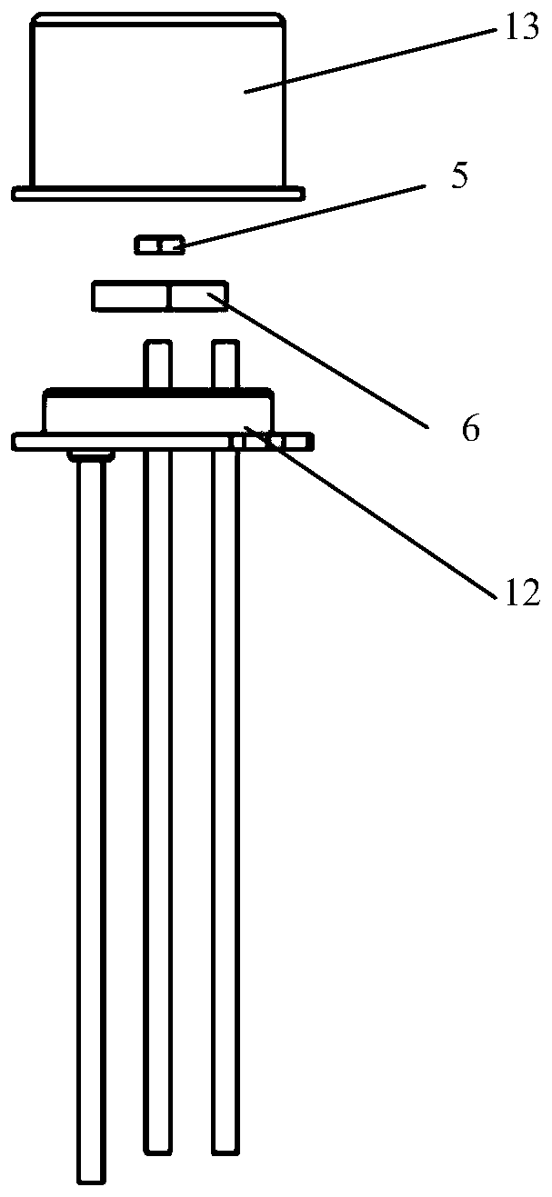
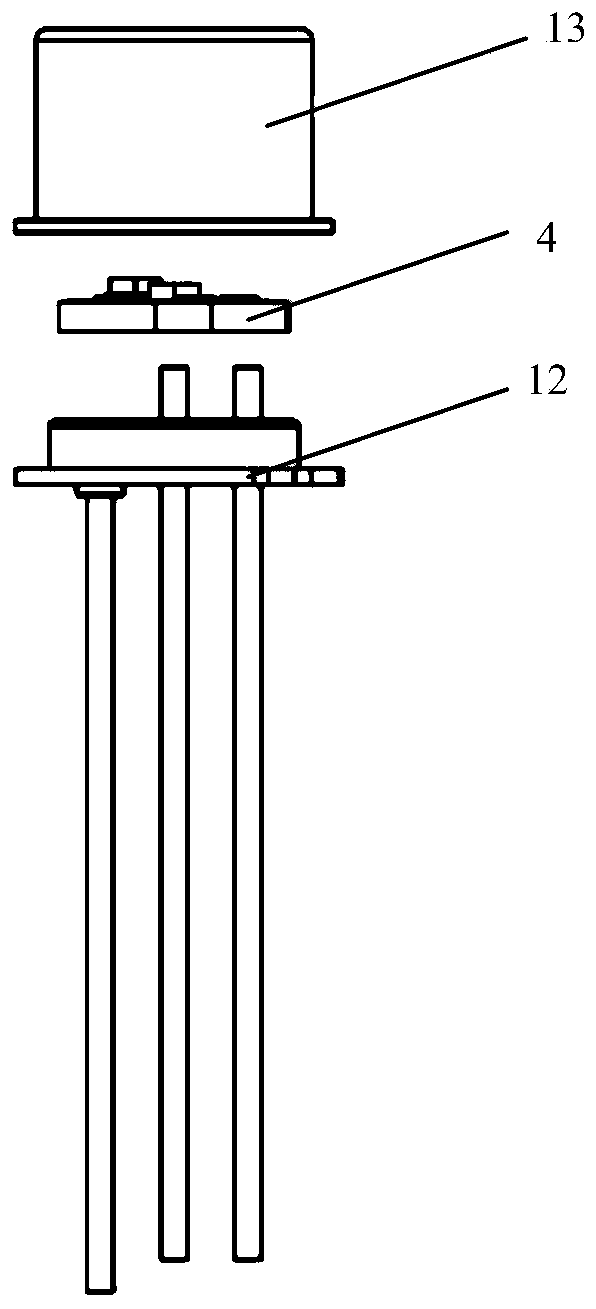
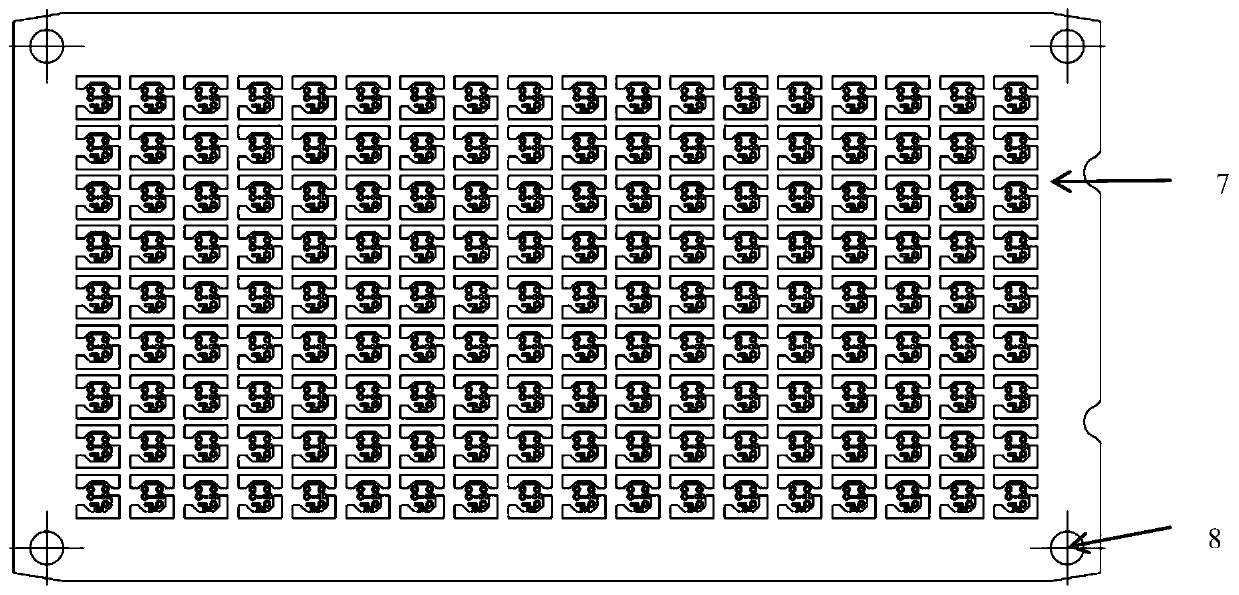
[0046] Step 1: Make a PCB board 7 composed of a skeleton and several small PCB boards 4 arranged on the skeleton, fix components on each of the small PCB boards 4, and connect the components with the corresponding The PCB small board 4 is welded;

[0047] Such as image 3 and Figure 7 As shown, in this embodiment, the components...


PUM


Abstract

The invention relates to a semiconductor device mixed packaging method which comprises the steps of making PCB formed by a skeleton and a plurality of mini PCBs arranged on the skeleton, wherein each mini PCB corresponds to a fixed component, and the components and corresponding mini PCBs are welded together, placing the PCB on the upper surface of a clamp with a plurality of pedestals arranged therein, allowing the pedestals in the clamp to be corresponded to the mini PCB on the PCB one to one, fixing the mini PCBs with corresponding pedestals, separating all mini PCBs from the PCB, so that the mini PCBs stay on the upper surface of corresponding pedestals, and the mini PCBs and the pedestals correspond one to one to form semi-finished pedestals, covering pipe cap on each semi-finished pedestal, and fixing the pipe caps with corresponding semi-finished pedestals. Components are directly processed on PCB, thereby simplifying production process. The semiconductor device mixed packaging method is suitable for mass production, and improves production efficiency. A chip-on-board packaging COB process is employed. The gild layer thickness at the welding point is small enough. The cost is saved, while ensuring quality.

Description

technical field [0001] The invention relates to the technical fields of optical communication and optical sensing devices, in particular to a hybrid packaging method for semiconductor devices. Background technique [0002] Due to the small size of the bare chip, fragile, and easy to be polluted, in order to make full use of the high performance of these semiconductor components and prevent them from being damaged by the external environment, we need to reasonably arrange the bare chip and other components on the frame and PCB board and Seal it. A good packaging method design is very important. It can not only give full play to the performance of the component itself, but also improve the reliability of the component, and also affect the design, production and manufacture of the circuit board it is connected to. The packaging of semiconductor devices has the following functions: one is physical protection, which protects components from the influence and damage of the extern...

Claims


Application Information

Patent Timeline
Patent Type & Authority Patents(China)
IPC IPC(8): H01L21/56H01L25/16H05K3/00H05K3/34
CPCH01L21/56H01L25/167H05K3/0008H05K3/3421H05K3/3457H05K3/3494
Inventor 李军蒋星
Owner 湖南赛尔光电科技有限公司
Features
  • Generate Ideas
  • Intellectual Property
  • Life Sciences
  • Materials
  • Tech Scout
  • Unparalleled Data Quality
  • Higher Quality Content
  • 60% Fewer Hallucinations
Learn More