Micro LED device and manufacturing method thereof

A technology of LED devices and manufacturing methods, which is applied to semiconductor devices, electric solid devices, instruments, etc., can solve problems such as complexity, long process flow, and inability to achieve micron levels, and achieve the effect of convenient operation and simple method

Active Publication Date: 2017-12-15
ANHUI SANAN OPTOELECTRONICS CO LTD
View PDF5 Cites 6 Cited by
  • Summary
  • Abstract
  • Description
  • Claims
  • Application Information

AI Technical Summary

Problems solved by technology

The process flow is long and complicated, and with the increase of the process, the relative risk of abnormality also increases
[0003] At present, the commonly used displays are often LCD displays, and OLED displays are more advantageous, but their pixel distances are all at the millimeter level, which cannot be achieved at the micron level.

Method used


Image

  • Micro LED device and manufacturing method thereof
  • Micro LED device and manufacturing method thereof
  • Micro LED device and manufacturing method thereof

Examples


Embodiment 1

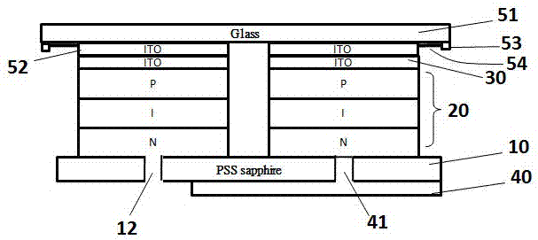
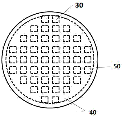
[0043] See attached figure 1 In one aspect, the present invention discloses a micro LED device, which at least includes a substrate 10, a plurality of LED elements arranged at intervals on the substrate 10, a plurality of LED elements share a substrate 10, and are periodically arranged on the substrate 10 on (eg figure 2 As shown), there are a plurality of through holes 12 penetrating the substrate at positions corresponding to the LED elements inside the substrate 10, and a metal back plate 40 is provided on the back of the substrate 10, and the metal back plate 40 has a plurality of protrusions corresponding to the through holes 12. The protrusion 41 is inserted into the through hole 12 and is electrically connected to the epitaxial wafer 20, and a transparent cover plate 50 is placed on the surface of the LED element. The material of the substrate 10 can be sapphire, silicon carbide, silicon, etc., and can be a patterned substrate, or a flat substrate. In this embodiment,...

Embodiment 2

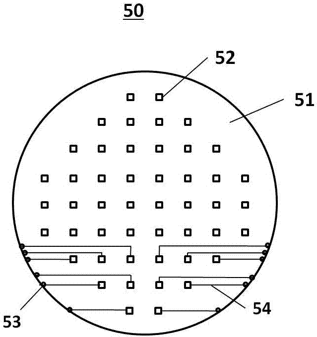
[0063] See attached Image 6 In this embodiment, in order to improve the heat dissipation effect of the micro-LED device, the metal backplane 40 may be configured to be composed of a plurality of electrically isolated sub-metal backplanes 42 . Each sub-metal backplane 42 corresponds to each LED element, conductive spacer 52 , metal contact 53 , and conductive wire 54 , with the same number.

[0064] In the micro-LED device, each metal contact 53 corresponds to an LED element and a sub-metal backplane 42, therefore, equivalent to a parallel structure of LED elements, the light emission of a single LED element can be individually controlled.


PUM

PropertyMeasurementUnit
Widthaaaaaaaaaa

Abstract

The invention provides a micro LED device and a manufacturing method thereof. According to the invention, a micron-scale LED element is manufactured with plasmas directly etched on an epitaxial wafer so that the LED element does not need to be transferred and that the substrate does not need to be stripped, and the inner part of the substrate is provided with a hole directly to form a through hole with the result that a metal back plate serving as a negative electrode penetrates through the through hole to be directly in contact with the epitaxial wafer; and when the through hole is manufactured on the substrate, a method combining the longitudinal multi-time invisible cutting and the laser scribing is utilized, which is simple and convenient to operate. In the invention, a metal contact located on the periphery of a transparent upper cover plate is designed as a positive electrode, and the direct connection of the positive electrode to the negative electrode is able to realize the illumination of the point-controlled LED element, so that a micro-scale small-size LED element does not need to be subjected to wire marking and transferring operation.

Description

technical field [0001] The invention belongs to the field of micro-LED devices, and in particular relates to a micro-LED device manufactured by epitaxial-level welding and a manufacturing method thereof. Background technique [0002] The current GaN chip manufacturing process is to first cover the core grain pattern on the epitaxial wafer, and then etch and plate the electrodes. Finally, individual core particles are split out for use. The process flow is long and complicated, and with the increase of the process, the relative risk of abnormality also increases. [0003] At present, the commonly used displays are often LCD displays, and OLED displays are more advantageous, but the pixel distances are all at the millimeter level, which cannot be achieved at the micron level. And MicroLED can reduce the pixel distance of the display to the micron level. Micro LED display, that is, LED miniaturization and matrix technology. It refers to a high-density micro-sized LED array ...

Claims


Application Information

Patent Timeline
IPC IPC(8): H01L27/15H01L33/00H01L33/62G09F9/33
CPCG09F9/33H01L27/156H01L33/0012H01L33/0075H01L33/62
Inventor 蔡家豪郑烨陈文志钟丹丹刘晶邱智中张家宏
Owner ANHUI SANAN OPTOELECTRONICS CO LTD
Why Eureka
Try Eureka