Metal grid electrode preparation method of 3D NAND memory

A metal gate and memory technology, applied in the field of metal gate preparation, can solve the problems of gaps in metal gates, affecting the performance of storage devices, hindering subsequent metal dielectric filling, etc., to achieve the effect of reducing possibility and improving performance

Active Publication Date: 2017-12-22
YANGTZE MEMORY TECH CO LTD
View PDF3 Cites 3 Cited by
  • Summary
  • Abstract
  • Description
  • Claims
  • Application Information

AI Technical Summary

Problems solved by technology

[0005] This "match head" structure leads to a reduction in the opening of the subsequent metal dielectric filling, thus hindering the filling of the subsequent metal dielectric, which easily leads to the presence of voids inside the formed metal gate, which ultimately affects the performance of the storage device

Method used


Image

  • Metal grid electrode preparation method of 3D NAND memory
  • Metal grid electrode preparation method of 3D NAND memory
  • Metal grid electrode preparation method of 3D NAND memory

Examples


Embodiment Construction

[0027] In order to reduce the influence of the by-product silicon dioxide on the subsequent filling of the metal medium, the embodiments of the present application try to remove the by-product silicon dioxide before filling the metal medium. Based on this, the present application provides a specific implementation of a method for preparing a metal gate of a 3D NAND memory.

[0028] see Figure 2 to Figure 3D . The metal gate preparation method of the 3D NAND memory provided in the embodiment of the present application includes the following steps:

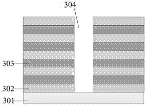
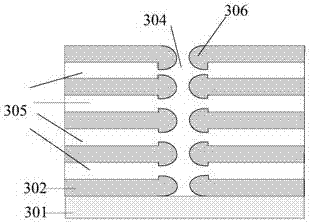
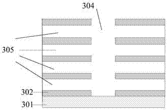
[0029] S201: Provide a substrate 301, on which a silicon oxide 302 / silicon nitride 303 alternate stack structure and a gate line slit (GLS) 304 passing through the stack structure are formed.

[0030] Such as Figure 3A As shown, a substrate 301 is provided, on which a silicon oxide 302 / silicon nitride 303 layer alternate stack structure and gate line gaps 304 passing through the stack structure are formed.

[0031] After the s...


PUM


Abstract

The invention provides a metal grid electrode preparation method of a 3D NAND memory. The metal grid electrode preparation method of a 3D NAND memory comprises steps of providing a substrate, wherein a silicon oxide layer / silicon nitride layer alternative staking structure and a grid line gap going through the silicon oxide layer / silicon nitride layer alternative stacking structure are formed on the substrate, adopting an etching solution with a selection ratio of the silicon nitride to the silicon oxide greater than 1 to etch the silicon nitride layer in the silicon oxide layer / silicon nitride layer alternative staking structure, forming a hollowed area in a 303 position of the silicon nitride layer, removing silicon dioxide which is a side product during the silicon nitride layer etching process, and filling the hollow area with a metal medium to form the metal grid electrode. The metal grid electrode preparation method of the 3D NAND memory can remove the side product silicon dioxide which is generated during the process of etching the silicon nitride before filling with metal medium. As a result, the opening of the position filled with the metal medium is not blocked by the side product, and the opening of the area filled with the metal medium is not reduced. The metal grid electrode preparation method of the 3D NAND memory reduces the possibility of forming an gap inside the metal grid electrode and can improve the performance of the 3D NAND memory.

Description

technical field [0001] The present application relates to the technical field of semiconductor processing, in particular to a method for preparing a metal gate of a 3D NAND memory. Background technique [0002] The vertical storage structure of the existing 3D NAND storage device is formed by stacking multi-layer dielectric films. During its preparation, it is necessary to remove the silicon nitride in the alternate stacked structure of silicon oxide / silicon nitride and fill it with a metal medium to form a metal dielectric. grid. [0003] At present, the removal of silicon nitride in the silicon oxide / silicon nitride alternating stacked structure is generally accomplished by a wet etching process. The wet etching solution gradually diffuses from the gate line slit (GLS) to the inside of the stacked structure, so as to gradually remove the silicon nitride in the stacked structure. [0004] However, in the existing wet etching process for removing silicon nitride, phosphori...

Claims


Application Information

Patent Timeline
Patent Type & Authority Applications(China)
IPC IPC(8): H01L21/28H01L27/11578
CPCH01L21/28H10B43/20
Inventor 张静平蒋阳波宋冬门吴良辉游晓英
Owner YANGTZE MEMORY TECH CO LTD
Why Eureka
Try Eureka