Preparation method of array substrate, array substrate and display device

An array substrate and substrate technology, which is applied in the field of optoelectronic display, can solve the problems of low utilization rate of light output, difficulty in guaranteeing product yield, and inability to support random bending.

Inactive Publication Date: 2017-12-26
BOE TECH GRP CO LTD
View PDF5 Cites 12 Cited by
  • Summary
  • Abstract
  • Description
  • Claims
  • Application Information

AI Technical Summary

Problems solved by technology

The flexible direction needs to continuously reduce the thickness of the OLED display panel. At present, the OLED substrate can achieve a thickness of about 100um, but in order to reduce the reflectivity, it is necessary to paste a circular polarizer, which leads to an increase in the overall thickness and cannot support random bending. Therefore, in orde...

Method used


Image

  • Preparation method of array substrate, array substrate and display device
  • Preparation method of array substrate, array substrate and display device
  • Preparation method of array substrate, array substrate and display device

Examples


Embodiment 1

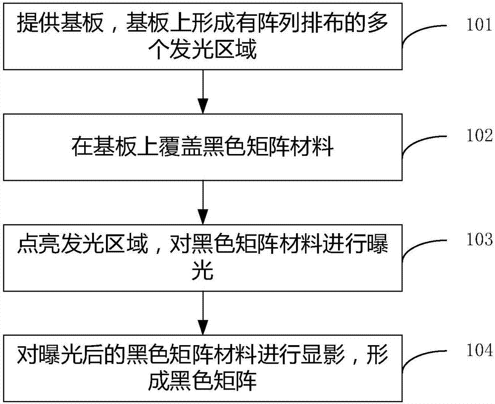
[0071] refer to figure 1 , which shows a flow chart of the steps of a method for preparing an array substrate provided in Embodiment 1 of the present invention, and the method may include:

[0072] Step 101: providing a substrate on which a plurality of light-emitting regions arranged in an array are formed.

[0073] Specifically, the substrate may include a plurality of light-emitting regions arranged in a pre-formed array, and there are many ways to provide the substrate. For example, the driving backplane may be fabricated using the existing technology, and then the organic light-emitting layer and the cathode may be fabricated on the driving backplane. layer to obtain a substrate, which may further include a thin film encapsulation layer formed on the surface of the cathode layer, refer to figure 2 , shows a schematic cross-sectional structure of the substrate.

[0074] Step 102: covering the black matrix material on the substrate.

[0075] Specifically, a black matrix...

Embodiment 2

[0084] refer to Figure 7 , shows a flow chart of steps of a method for providing a substrate provided in Embodiment 2, and the step of providing a substrate may include:

[0085] Step 201: Provide a driving backplane.

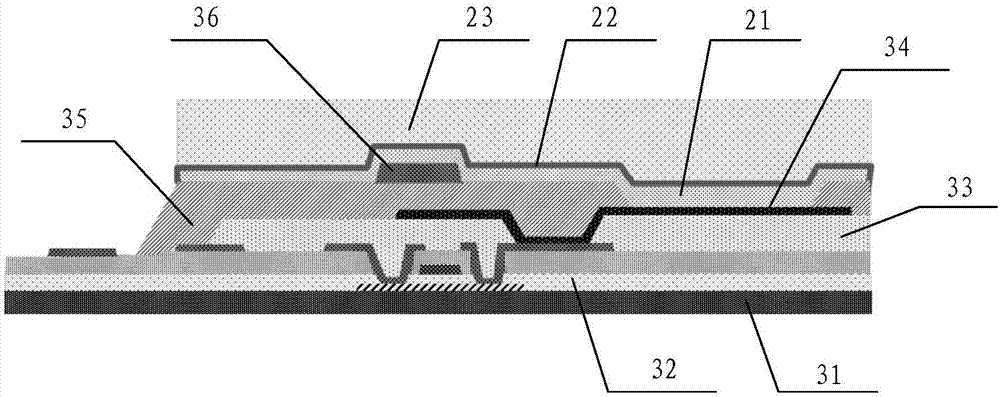
[0086] Specifically, there are many methods for providing a driving backplane, which are not limited in this application. Refer to Figure 8 , shows a schematic cross-sectional structure of a driving substrate.

[0087] Step 202: Form the organic light-emitting layer 21 and the cathode layer 22 on the driving backplane to obtain the substrate.

[0088] Specifically, refer to Figure 9 , shows a schematic cross-sectional structure of the substrate after the organic light-emitting layer and the cathode layer are fabricated. The organic light emitting layer 21 can be formed on the driving backplane by means of vapor deposition, and then the cathode layer 22 can be formed on the organic light emitting layer 21 by means of vapor deposition or sputtering, so as ...

Embodiment 3

[0091] refer to Figure 10 , which shows a flow chart of steps for providing a substrate provided in Embodiment 3, and the step of providing a substrate may include:

[0092] Step 301: Provide a driving backplane.

[0093] Step 302: Form the organic light emitting layer 21 and the cathode layer 22 on the driving backplane.

[0094] Specifically, for the process methods of step 301 and step 302, reference may be made to the description in Embodiment 2, and details are not repeated here.

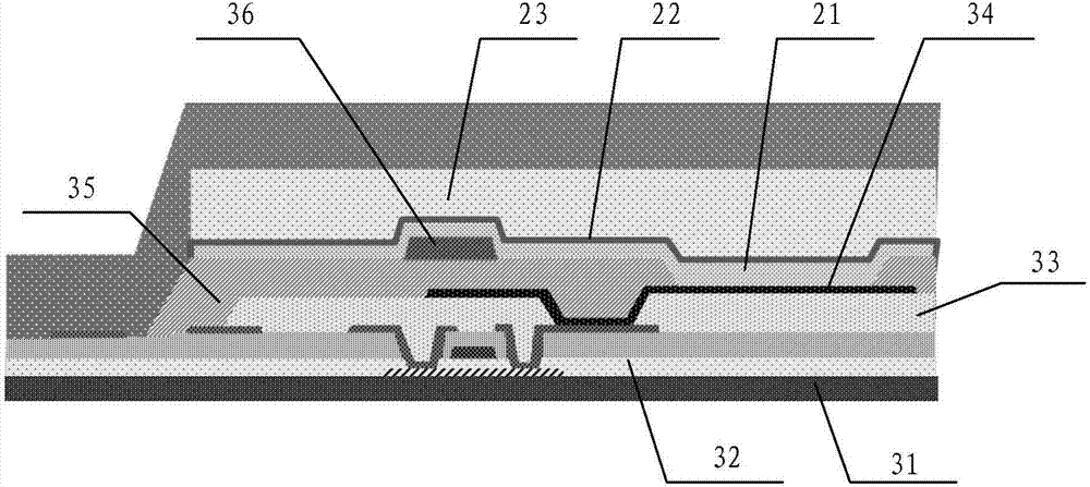
[0095] Step 303: forming a thin film encapsulation layer 23 on the cathode layer 22 to obtain a substrate.

[0096] Specifically, a thin film encapsulation layer 23 can also be formed on the cathode layer 22 to obtain a substrate, referring to figure 2 , shows a schematic cross-sectional structure diagram of the substrate on which the thin film encapsulation layer has been fabricated. The thin-film encapsulation layer 23 is used to protect the organic light-emitting layer 21 , prevent the...


PUM


Abstract

The invention provides a preparation method of an array substrate, the array substrate and a display device. According to the preparation method, exposure of a black matrix material is achieved by lightening a luminous area on the substrate, and thus the exposed black matrix material is developed to obtain a black matrix. The black matrix material at a corresponding position is exposed by adopting its luminous area, self alignment is achieved, the alignment deviation problem between the black matrix and the luminous area is avoided, and accordingly the emergent light utilization rate is improved. In addition, the made black matrix can replace a circular polarizer to reduce the reflection rate of a display panel, and accordingly the flexibility of the display panel is ensured. Furthermore, the preparation method also gets rid of the limitations of an existing process evaporation mask, and the product resolution can be thus improved.

Description

technical field [0001] The invention relates to the field of photoelectric display technology, in particular to a method for preparing an array substrate, an array substrate and a display device. Background technique [0002] At present, the share of OLED display products in small-size products is getting higher and higher, and there are also products emerging in the medium-size class. It is foreseeable that the development will continue to accelerate in the future. The main development direction of OLED display products in the future is flexibility and ultra-high resolution. The flexible direction needs to continuously reduce the thickness of the OLED display panel. At present, the OLED substrate can achieve a thickness of about 100um, but in order to reduce the reflectivity, it is necessary to paste a circular polarizer, which leads to an increase in the overall thickness and cannot support random bending. Therefore, in order to reduce the reflection To ensure product fle...

Claims


Application Information

Patent Timeline
IPC IPC(8): H01L27/12H01L21/77
CPCH01L27/1214H01L27/1259H10K59/38H10K59/123H10K59/131H10K50/865H10K59/1201H10K50/844H10K59/12H10K71/00
Inventor 舒适徐传祥卢江楠
Owner BOE TECH GRP CO LTD
Why Eureka
Try Eureka