SOI-based MOS device structure and manufacturing method thereof

A technology of MOS devices and manufacturing methods, which is applied in semiconductor/solid-state device manufacturing, semiconductor devices, electrical components, etc., can solve problems such as increased leakage, achieve the effects of ensuring effective width, simple manufacturing process, and suppressing total dose effect

Active Publication Date: 2017-12-26
SHANGHAI INST OF MICROSYSTEM & INFORMATION TECH CHINESE ACAD OF SCI
View PDF5 Cites 8 Cited by
  • Summary
  • Abstract
  • Description
  • Claims
  • Application Information

AI Technical Summary

Problems solved by technology

[0009] In view of the above-mentioned shortcomings of the prior art, the object of the present invention is to provide a SOI-based MOS device structure and its manufacturing method, which is used to solve the problem of increased leakage of SOI MOS devices in the prior art due to the total dose effect

Method used


Image

  • SOI-based MOS device structure and manufacturing method thereof
  • SOI-based MOS device structure and manufacturing method thereof
  • SOI-based MOS device structure and manufacturing method thereof

Examples


Embodiment 1

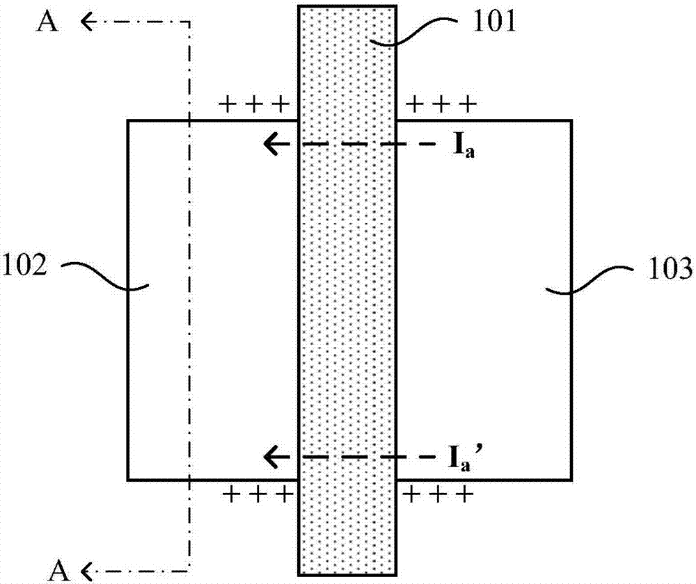
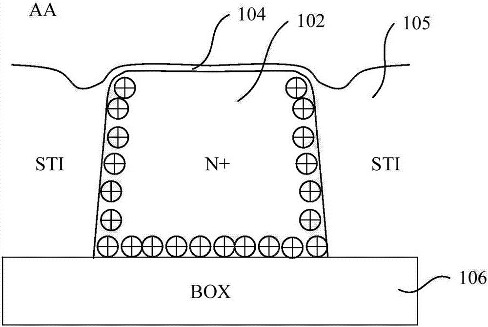
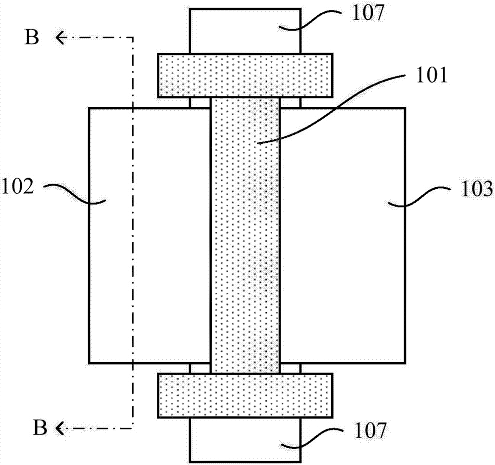
[0065] The present invention provides a kind of SOI-based MOS device structure, please refer to Figure 5 to Figure 11 , which are respectively shown as a top view and a C-C, D-D, E-E, and F-F sectional view of the SOI-based MOS device structure. As shown in the figure, the SOI-based MOS device structure includes a back substrate 205, an insulating buried layer 206 on the back substrate 205, an active region on the insulating buried layer 206, and surrounding the active region. A shallow trench isolation structure 207 in the source region; wherein:

[0066] A MOS device is formed in the active region, and the MOS device includes a gate region 201, a body region 208 located under the gate region 201, and a first conductivity type source region 202 located on the first lateral side of the body region 208 and the drain region 203 of the first conductivity type located on the second lateral side of the body region 208; wherein: both ends of the gate region 201 extend toward the s...

Embodiment 2

[0083] The present invention also provides a method for fabricating an SOI-based MOS device structure, comprising the steps of:

[0084] First execute step S1: Figure 12 As shown, an SOI substrate including a back substrate 205, an insulating buried layer 206, and a top layer of silicon is provided in order from bottom to top, and a shallow trench isolation structure 207 is formed in the top layer of silicon to isolate an active region.

[0085] As an example, both the back substrate 205 and the top layer silicon are P-type Si.

[0086] Then execute step S2: as Figure 13 As shown, the gate region 201 of the MOS device is formed on the active region; both ends of the gate region 201 extend toward the second lateral side thereof, forming an "L"-shaped bending angle (such as Figure 5 or Figure 6 shown); the active region below the gate region 201 constitutes the body region of the MOS device.

[0087] Specifically, the gate region 201 includes a gate dielectric layer 2011...


PUM


Abstract

The invention provides an SOI-based MOS device structure and a manufacturing method thereof. The structure comprises a backing bottom, an insulation buried layer, an active region and a shallow trench isolation structure, wherein an MOS device is formed in the active region, the MOS device comprises a grid region, a body region under the grid region, a first conductive type source region on the first lateral side in the body region and a second conductive type drain region on the second lateral side of the body region. The two ends of the grid region extend in the second lateral side direction to form an L-shaped bending corner. The active region further comprises a second conductive type body contact region, which is in contact with the body region and encloses the two vertical ends and bottom portion of the active region. The doping density of the contact region is greater than that of the body region. Box power leakage, upper and lower corner power leakage and sidewall power leakage due to the total dose effect of SOI device, the effective width of the source region can be ensured, and the driving capacity of the device may not be damaged.

Description

technical field [0001] The invention belongs to the technical field of semiconductor manufacturing, and relates to an SOI-based MOS device structure and a manufacturing method thereof. Background technique [0002] SOI (Silicon-On-Insulator) refers to silicon on insulator. Since its invention, SOI technology has been applied to the field of semiconductor manufacturing due to its natural anti-single event latch-up effect, small parasitic capacitance, high integration, and low power consumption. Aerospace electronic components are widely used due to their advantages of anti-single event effect compared with bulk silicon. [0003] Due to the harsh working environment of aerospace electronic components, the performance of the device is often affected by particle radiation; the most common ones are the total dose effect and the single event effect. Compared with the bulk silicon process, SOI devices add a layer of BOX insulating layer between the top silicon and the substrate, ...

Claims


Application Information

Patent Timeline
Patent Type & Authority Applications(China)
IPC IPC(8): H01L29/78H01L29/423H01L21/336H01L21/28
CPCH01L29/42356H01L29/66568H01L29/78
Inventor 陈静何伟伟罗杰馨王曦
Owner SHANGHAI INST OF MICROSYSTEM & INFORMATION TECH CHINESE ACAD OF SCI
Why Eureka
Try Eureka