Semiconductor device, manufacture method for the same and electronic device

A manufacturing method and semiconductor technology, applied in the direction of semiconductor devices, electric solid devices, circuits, etc., can solve problems such as high difficulty, increased cost, and increased device manufacturing cost, and achieve low cost, reduced manufacturing cost, and reduced manufacturing process difficulty Effect

Active Publication Date: 2018-01-05
SEMICON MFG INT (SHANGHAI) CORP +1
View PDF3 Cites 3 Cited by
  • Summary
  • Abstract
  • Description
  • Claims
  • Application Information

AI Technical Summary

Problems solved by technology

With people's pursuit of storage capacity, it is necessary to manufacture larger-capacity memories, and it is also necessary to manufacture more layers of control gates. If the number of layers increases to, for example, 128 layers or more multiples of layers, in such a structure, the same step It is very difficult to make through holes with different depths in the process, and the step structure control gate structure and contact plugs increase the cost per bit. In addition, it is necessary to make the step structure control gate structure and contact plugs. Requires many steps of photolithography process, which correspondingly increases the fabrication cost of the device

Method used


Image

  • Semiconductor device, manufacture method for the same and electronic device
  • Semiconductor device, manufacture method for the same and electronic device
  • Semiconductor device, manufacture method for the same and electronic device

Examples


Embodiment 1

[0050] The following will refer to Figure 3A ~ Figure 3D A method for fabricating a semiconductor device according to an embodiment of the present invention will be described in detail.

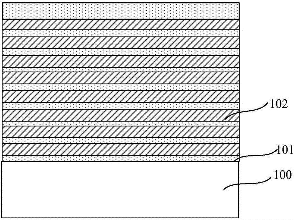
[0051] First, if Figure 3A As shown, a semiconductor substrate 300 is provided. The semiconductor substrate 300 is at least divided into a storage area and a contact plug area. A multilayer stack structure is formed on the semiconductor substrate in the storage area, and each stack structure includes a dielectric layer. 301 and the control gate layer 302 above the dielectric layer 301 . A first dielectric layer 303 covering the multilayer stack structure and the contact plug region is formed on the semiconductor substrate 300, and a patterned hard mask is formed on the first dielectric layer 303 Layer 304.

[0052] Wherein, the semiconductor substrate 300 can be at least one of the materials mentioned below: Si, Ge, SiGe, SiC, SiGeC, InAs, GaAs, InP or other III / V compound semiconductors...

Embodiment 2

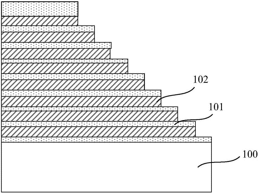
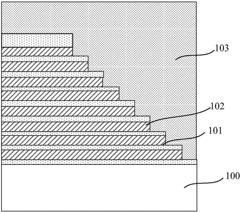
[0071] The present invention also provides a semiconductor device fabricated by the above method, such as Figure 4 As shown, the semiconductor device includes: a semiconductor substrate 400, the semiconductor substrate 400 is at least divided into a storage area and a contact plug area, a multi-layer stack structure is formed on the semiconductor substrate in the storage area, each stack The layer structure includes a dielectric layer 401 and a control gate layer 402 located above the dielectric layer 401; a first dielectric layer 403, the first dielectric layer 403 covers the multi-layer stack structure and the contact plug area, in the A plurality of first contact plugs 404 corresponding to the control gate layers in the multilayer stack structure are formed in the first dielectric layer 403 in the contact plug region, and the first contact plugs 404 are formed by each The control gate layer extends obliquely to the upper surface of the first dielectric layer 403; the secon...

Embodiment 3

[0079] Still another embodiment of the present invention provides an electronic device, including a semiconductor device and an electronic component connected to the semiconductor device. Wherein, the semiconductor device includes: a semiconductor substrate, the semiconductor substrate is at least divided into a storage area and a contact plug area, a multi-layer stack structure is formed on the semiconductor substrate in the storage area, and each stack structure includes A dielectric layer and a control gate layer located above the dielectric layer; a first dielectric layer, the first dielectric layer covers the multilayer stack structure and the contact plug area, and the first contact plug area in the contact plug area A plurality of first contact plugs corresponding to the control gate layers in the multi-layer stack structure are formed in a dielectric layer, and the first contact plugs extend obliquely from each of the control gate layers to the first The upper surface ...


PUM


Abstract

The invention provides a semiconductor device, a manufacture method for the same and an electronic device. The manufacture method for the semiconductor device comprises steps of providing a semiconductor substrate, wherein the semiconductor substrate at least comprises a storage area and a contact plugging area, forming multiple layers of laminating structures on the semiconductor substrate in thestorage area and each laminating layer structure comprises a dielectric layer and a control gate layer arranged over the dielectric layer, forming a first dielectric layer covering the multiple layers of laminating layer structures and the contact plugging area, forming multiple first contact plugs which correspond to the control gate layer in the multiple layers of laminating layers in the firstdielectric layer in the contact plugging area, forming a second dielectric layer on the first dielectric layer and forming multiple second contact plugs which are in corresponding connection with multiple first contact plugs in the second dielectric layer. The manufacture method can reduce technology difficulty and cost and the semiconductor device and the electronic device are simple in structure and low in cost.

Description

technical field [0001] The present invention relates to the technical field of semiconductors, in particular to a semiconductor device, a manufacturing method thereof, and an electronic device. Background technique [0002] With the development of semiconductor process technology and the industry's demand for memory with high integration density and large storage capacity, 3D NAND (three-dimensional NAND) memory has emerged as the times require. A 3D NAND structure such as Figure 6 As shown, it includes a multi-layer storage array 1, the bottom selection gate LS (Lower SG) and the source line SL (Source Line) below the displacement storage array 1, the top selection gate US (Upper SG) above the storage array 1, The bit line BL (Bit Line) located above the select gate on the top layer, and the control gate CG (Control Gate) extending from each layer of the memory array 1 . For each layer of memory, it extends from the control gate of this layer, and is connected to the cont...

Claims


Application Information

Patent Timeline
Patent Type & Authority Applications(China)
IPC IPC(8): H01L27/11548H01L27/11575
Inventor 张海洋常荣耀郑喆
Owner SEMICON MFG INT (SHANGHAI) CORP
Why Eureka
Try Eureka