PCB (Printed Circuit Board) component and light emitting component

A technology of light emitting components and PCB boards, applied in the field of communication, can solve the problems of high gold wire arch, large high frequency loss, poor transmission characteristics, etc., and achieve small gold wire arch height, low high frequency loss, and good transmission characteristics Effect

Inactive Publication Date: 2018-01-05
NEW H3C TECH CO LTD
View PDF7 Cites 10 Cited by
  • Summary
  • Abstract
  • Description
  • Claims
  • Application Information

AI Technical Summary

Problems solved by technology

[0003] The purpose of the present disclosure is to provide a PCB board assembly, which aims to at least partially solve the problem that the height difference between the driver chip on the existing PCB board and the PCB substrate is too large, resulting in a high height of the gold wire interconnection between the two. The technical problem of large frequency loss and poor transmission characteristics
[0004] The purpose of the present disclosure is to also provide a light emitting component, which aims to at least partially solve the technical problems of the existing optical module transmitting component with large high-frequency loss and poor transmission characteristics

Method used


Image

  • PCB (Printed Circuit Board) component and light emitting component
  • PCB (Printed Circuit Board) component and light emitting component
  • PCB (Printed Circuit Board) component and light emitting component

Examples


no. 1 example

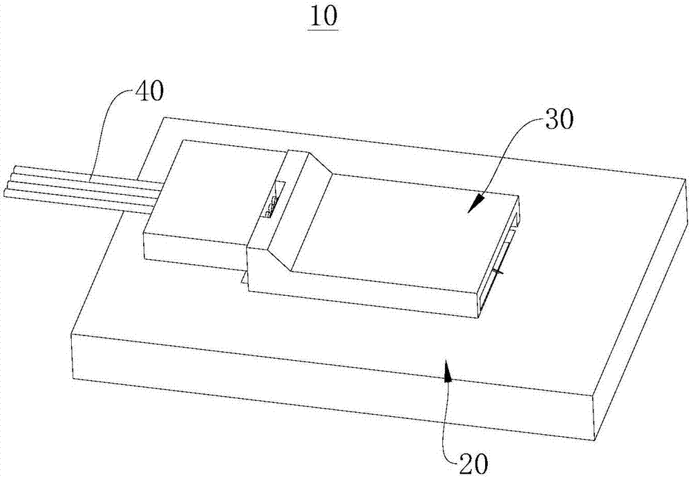
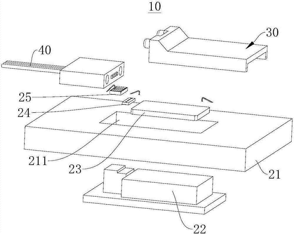
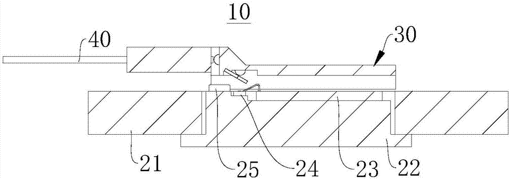
[0033] see Figure 1 to Figure 3 , the present embodiment provides a light emitting assembly 10, the light emitting assembly 10 includes a lens assembly 30 and a PCB board assembly 20, the PCB board assembly 20 includes a PCB substrate 21, a step gasket 22, a driver chip 23, a laser chip 24 and a monitoring The chip 25 and the PCB substrate 21 are provided with a mounting hole 211 , the mounting hole 211 is a through hole, and the step gasket 22 is assembled in the mounting hole 211 . The step spacer 22 includes a top surface constituting a mounting surface. The driver chip 23, the laser chip 24 and the monitoring chip 25 are all mounted on the mounting surface. The lens assembly 30 is arranged on the PCB board assembly 20, and the optical fiber 40 is connected to the lens assembly 30. The lens assembly 30 is used to divide the light emitted by the laser chip 24 into two paths of light directed to the monitoring chip 25 and the optical fiber 40 respectively.

[0034] The mon...

no. 2 example

[0059] This embodiment provides a light emitting assembly 10, which is similar in structure to the light emitting assembly 10 in the first embodiment, except that the structure of the PCB board assembly 20 is different.

[0060] see Figure 9 , in the PCB board assembly 20 provided by this embodiment, the mounting surface of the step gasket 22 only includes the first surface 221 and the second surface 222, the laser chip 24 is located on the first surface 221 of the step gasket 22, and the driver chip 23 is located on the first surface 221 of the step gasket 22. The second surface 222 of the step washer 22 . The height of the first surface 221 is higher than that of the second surface 222 , so that the height difference between the top surface of the driver chip 23 and the top surface of the laser chip 24 and the top surface of the PCB substrate 21 is smaller than the thickness of the driver chip 23 .

[0061] The monitoring chip 25 is mounted on the surface of the PCB substr...

no. 3 example

[0064] This embodiment provides a light emitting assembly 10, which is similar in structure to the light emitting assembly 10 in the first embodiment, except that the structure of the PCB board assembly 20 is different.

[0065] see Figure 10 , in the PCB assembly 20 provided in this embodiment, the mounting hole 211 is a blind hole, and the bottom of the mounting hole 211 is a mounting surface. The installation surface only includes the first surface 221 and the second surface 222 , the laser chip 24 is located on the first surface 221 of the stepped spacer 22 , and the driver chip 23 is located on the second surface 222 of the stepped spacer 22 . The height of the first surface 221 is higher than that of the second surface 222 , so that the height difference between the top surface of the driver chip 23 and the top surface of the laser chip 24 and the top surface of the PCB substrate 21 is smaller than the thickness of the driver chip 23 .

[0066] The monitoring chip 25 i...


PUM


Abstract

The invention provides a PCB (Printed Circuit Board) component and a light emitting component, and relates to the technical field of communication. The PCB component comprises a PCB substrate and a driving chip, wherein a mounting hole is formed in the PCB substrate; a mounting surface is arranged at the bottom of the mounting hole; the driving chip is arranged on the mounting surface; and a height difference between the top surface of the driving chip and the top surface of the PCB substrate is less than the thickness of the driving chip. Therefore, the height difference between the top surface of the driving chip and the top surface of the PCB substrate is smaller; the arch height formed by gold wire bonding connection between the top surface of the driving chip and the top surface of the PCB substrate is lower; the high-frequency loss of the PCB component is lower; and the transmission characteristic is good.

Description

technical field [0001] The present disclosure relates to the technical field of communication, and relates to a PCB board assembly and a light emitting assembly. Background technique [0002] At present, 4*10G and 4*25G short-distance communication optical module transmitting components adopt 4-channel Vcsel (Vertical Cavity Surface Emitting Laser, Chinese translation: "Vertical Cavity Surface Emitting Laser") parallel emission structure. Installed on the PCB board, the external lens assembly is used to arrange the optical path and then coupled to the optical fiber. Contents of the invention [0003] The purpose of the present disclosure is to provide a PCB board assembly, which aims to at least partially solve the problem that the height difference between the driver chip on the existing PCB board and the PCB substrate is too large, resulting in a high height of the gold wire interconnection between the two. The technical problem of large frequency loss and poor transmis...

Claims


Application Information

Patent Timeline
Patent Type & Authority Applications(China)
IPC IPC(8): H01S5/022H01S3/02
Inventor 李贤杰
Owner NEW H3C TECH CO LTD
Why Eureka
Try Eureka