Hard connection implementation method of optical module and optical module

An implementation method and hard connection technology, applied in the field of optical communication, can solve problems such as large insertion loss of optical signals, large signal attenuation of optical modules, unqualified module indicators, etc., and achieve the goal of reducing high-frequency loss, avoiding defects, and high reliability Effect

Active Publication Date: 2021-11-02
LINKTEL TECH CO LTD
View PDF16 Cites 3 Cited by
  • Summary
  • Abstract
  • Description
  • Claims
  • Application Information

AI Technical Summary

Problems solved by technology

In order to meet the electrical interface and optical interface stipulated in the agreement, when the PCBA in the optical module and the optical port of the optical device are hard-connected, since the PCBA and the optical device are completed in the normal production process, that is, the optical device component is made first, Then assembled into the module, the various deviations formed by the optical device components will accumulate at the module end, resulting in deviations in the key high-frequency electrical signals and key optical paths during hard connections, which in turn lead to large attenuation of the optical module signal, The insertion loss of the optical signal is large, and the module index is unqualified in severe cases. At the same time, the hard connection will cause the mechanical stress of the PCBA and the optical device after assembly, which will affect the reliability of the later stage.

Method used


Image

  • Hard connection implementation method of optical module and optical module
  • Hard connection implementation method of optical module and optical module
  • Hard connection implementation method of optical module and optical module

Examples


Embodiment 1

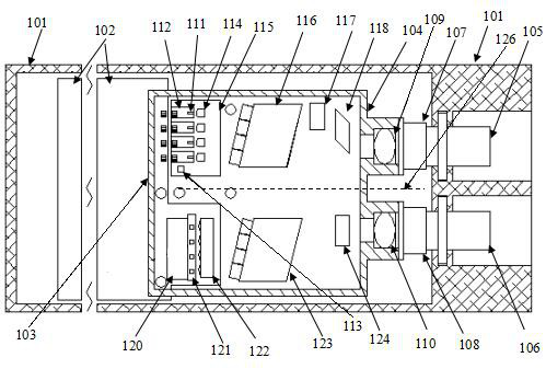
[0079] see Figure 1 to Figure 4 An embodiment of the present invention provides an optical module, including a module case 101, a PCBA 102, and an optical device 103. The optical device 103 includes a device case 104, a transmitting optical interface 105, a receiving optical interface 106, an adjustable sliding ring 107 at the transmitting end, Adjustable sliding ring 108 at the receiving end, optical port lens 109 at the transmitting end, optical port lens 110 at the receiving end, laser chipset 111, ceramic carrier group 112, thermistor 113, collimating lens group 114, TEC115, wavelength division multiplexing components 116 , an isolator 117 , a transmitter prism 118 , a detector chipset 119 , a TIA chip 120 , a triangular reflection prism 121 , an array lens 122 , a wave division multiplexing component 123 and a receiver prism 124 .

[0080] Among them, the transmitting optical interface 105, the adjustable sliding ring 107 at the transmitting end, the optical port lens 10...

Embodiment 2

[0090] see Figure 5 to Figure 11 , the embodiment of the present invention discloses a hard connection implementation method of an optical module, comprising the following steps:

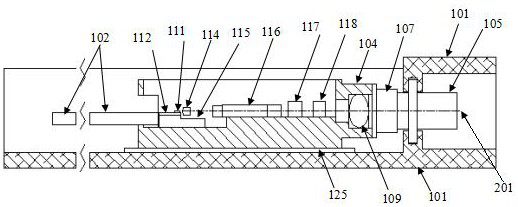
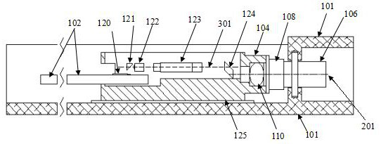
[0091] Step 1: fixing part of the transmitting-end optical element and part of the receiving-end optical element inside the device case to form a first assembly. Such as Figure 5 , Figure 6 As shown, in this step, passive optics such as the optical port lens 109 at the transmitting end, the optical port lens 110 at the receiving end, the wavelength division multiplexing component 116 and the prism 118 at the transmitting end are bonded inside the device casing 104 . The order of bonding is not limited.

[0092] It should be noted here that three circular holes 501 , 502 , and 503 are processed in the device case 104 , and the contours of the circular holes are used as marks. The positions of the circular holes 501, 502, and 503 are strongly related to the mounting positions of the optical win...


PUM

PropertyMeasurementUnit
radiusaaaaaaaaaa

Abstract

The invention relates to a hard connection implementation method of an optical module and the optical module, and the method comprises the steps: carrying out the hard connection, carrying out the integrated assembly of a PCBA and an optical device, and then carrying out the surface mounting of internal key elements, thereby avoiding the obvious dislocation of an optical path or a circuit; carrying out key high-frequency interconnection, carrying out light path interconnection by utilizing the characteristic that parallel light paths are insensitive to axial deviation and transverse deviation, forming a non-positive-sequence implementation method, thus the advantage of large light spot coupling tolerance can be compatible, each channel can be kept to be coupled to the optimal tolerance curve position, and meanwhile, the device is simple in structure, the coupling method is easy to control, and has the advantages of small occupied space, easy assembly and the like.

Description

technical field [0001] The invention belongs to the technical field of optical communication, and in particular relates to a hard connection realization method of an optical module and the optical module. Background technique [0002] For many miniaturized optical modules, such as SFP+ optical modules, QSFP+ optical modules, QSFP28 optical modules, etc., the optical device is assembled in the module by bending the TO pin of the optical device through a soft tape or assembled with the PCBA. , this method is common in the application of airtight optical devices, such as patents with application numbers CN201711243548.9, CN201710833529.5, CN201921371832.9, etc.; for the application of non-hermetic optical devices, especially the optical module is very small Optical modules such as SFP DD, QSFP DD and other packages, because the single rate reaches 100Gpbs and above, the corresponding PCBA is equipped with higher rate electrical chips, such as DSP chips, driver chips and other a...

Claims


Application Information

Patent Timeline
Patent Type & Authority Applications(China)
IPC IPC(8): G02B6/42
Inventor 胡百泉林雪枫李林科吴天书杨现文张健
Owner LINKTEL TECH CO LTD
Why Eureka
Try Eureka